EasyManua.ls Logo

Intel Embedded Intel486 User Manual

Intel Embedded Intel486
334 pages
To Next Page IconTo Next Page
To Previous Page IconTo Previous Page
Page #96 background imageLoading...
Page #96 background image
EMBEDDED Intel486 PROCESSOR HARDWARE REFERENCE MANUAL
4-32
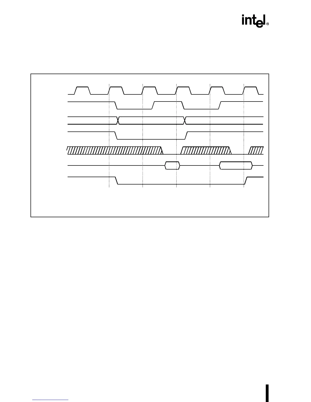
When LOCK# is asserted, the Intel486 processor recognizes address hold and backoff but does
not recognize bus hold. It is left to the external system to properly arbitrate a central bus when the
Intel486 processor generates LOCK#.
Figure 4-23. Locked Bus Cycle
4.3.7 Pseudo-Locked Cycles
Pseudo-locked cycles assure that no other master is given control of the bus during operand trans-
fers that take more than one bus cycle.
For the Intel486 processor, examples include 64-bit description loads and cache line fills.
Pseudo-locked transfers are indicated by the PLOCK# pin. The memory operands must be
aligned for correct operation of a pseudo-locked cycle.
PLOCK# need not be examined during burst reads. A 64-bit aligned operand can be retrieved in
one burst (note that this is only valid in systems that do not interrupt bursts).
The system must examine PLOCK# during 64-bit writes since the Intel486 processor cannot
burst write more than 32 bits. However, burst can be used within each 32-bit write cycle if BS8#
or BS16# is asserted. BLAST is de-asserted in response to BS8# or BS16#. A 64-bit write is driv-
en out as two non-burst bus cycles. BLAST# is asserted during both 32-bit writes, because a burst
is not possible. PLOCK# is asserted during the first write to indicate that another write follows.
This behavior is shown in Figure 4-24.
242202-080
TiT2T1T2T1Ti
CLK
ADS#
A31–A2
M/IO#
D/C#
BE3#–BE0#
W/R#
RDY#
DATA
LOCK#
To Processor
From Processor
Read Write

Table of Contents

Question and Answer IconNeed help?

Do you have a question about the Intel Embedded Intel486 and is the answer not in the manual?

Intel Embedded Intel486 Specifications

General IconGeneral
BrandIntel
ModelEmbedded Intel486
CategoryComputer Hardware
LanguageEnglish

Summary

Introduction

Processor Features

Details core features like 32-bit RISC core, pipelining, on-chip cache, and MMU.

On-chip Cache

Details the 8/16-Kbyte unified cache, its protocols, and line fills.

Internal Architecture

Instruction Pipelining

Explains how instructions are processed in stages for improved performance.

Cache Unit

Covers cache operation, including hits, misses, line fills, and update policies.

Bus Operation

Data Transfer Mechanism

Explains how data operands of various lengths are transferred over the bus.

Locked Cycles

Covers atomic memory access using the LOCK# pin for read-modify-write operations.

Memory Subsystem Design

Improving Write Cycle Latency

Covers techniques like interleaving and write posting to reduce write latency.

Second-Level Cache

Explains the advantages and performance benefits of using an L2 cache.

Peripheral Subsystem

System Bus Design

PCI BUS: SYSTEM DESIGN EXAMPLE

Introduces the PCI bus, its features, and its implementation in embedded systems.

Performance Considerations

Instruction Execution Performance

Reviews how Intel486 processors achieve faster instruction execution and compares with earlier processors.

Internal Cache Performance Issues

Analyzes the on-chip cache's organization, size, and impact on performance.

On-Chip Write Buffers

Details the function of write buffers in reducing latency and enhancing write performance.

Second-Level Cache Performance Considerations

Explains the advantages and performance benefits of using an L2 cache.

Floating-Point Performance

Analyzes the floating-point unit's performance, execution sequences, and on-chip interface.

Physical Design and System Debugging

Power Dissipation and Distribution

Discusses power dissipation, capacitive loading, and power/ground planes.

High-Frequency Design Considerations

Covers management of transmission lines, impedance control, and EMI.

Latch-Up

Covers prevention of latch-up by observing voltage limits and using proper layout.

Clock Considerations

Discusses requirements for clock signals, skew, and loading effects.

Thermal Characteristics

Explains thermal specifications, junction temperature calculation, and heatsink usage.

Building and Debugging the Intel486™ Processor-Based System

Outlines steps for building and debugging the system incrementally.

Related product manuals