EasyManua.ls Logo

Intel Embedded Intel486 User Manual

Intel Embedded Intel486
334 pages
To Next Page IconTo Next Page
To Previous Page IconTo Previous Page
Page #119 background image
4-55
BUS OPERATION
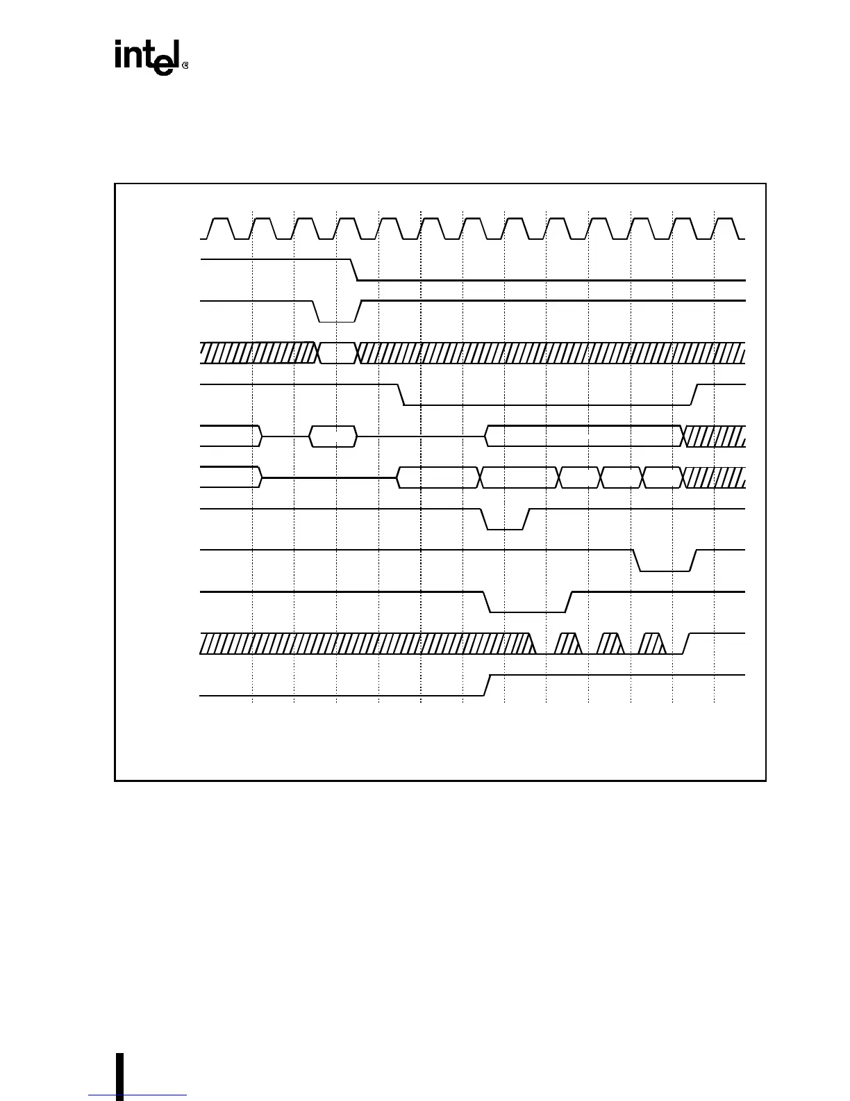
When a line is written back, KEN#, WB/WT#, BS8#, and BS16# are ignored, and PWT and PCD
are always low during write-back cycles.
Figure 4-38. Snoop Cycle Invalidating a Modified Line
The next ADS# for a new cycle can occur immediately after the last RDY# or BRDY# of the
write-back cycle. The Write-Back Enhanced IntelDX4 processor does not guarantee a dead clock
between cycles unless the second cycle is a snoop-forced write-back cycle. This allows snoop-
forced write-backs to be backed off (BOFF#) when snooping under AHOLD.
HITM# is guaranteed to remain asserted until the RDY# or BRDY# signals corresponding to the
last doubleword of the write-back cycle is returned. HITM# is de-asserted from the clock edge in
which the last BRDY# or RDY# for the snoop write-back cycle is asserted. The write-back cycle
could be a burst or non-burst cycle. In either case, 16 bytes of data corresponding to the modified
line that has a snoop hit is written back.
242202-150
CLK
AHOLD
EADS#
INV
HITM#
BRDY#
CACHE#
12345678910111213
BLAST#
A31–A4
*
**
A3–A2 0 4 8 C
ADS#
W/R#
To Processor
Write-back from Processor
*
**

Table of Contents

Question and Answer IconNeed help?

Do you have a question about the Intel Embedded Intel486 and is the answer not in the manual?

Intel Embedded Intel486 Specifications

General IconGeneral
BrandIntel
ModelEmbedded Intel486
CategoryComputer Hardware
LanguageEnglish

Summary

Introduction

Processor Features

Details core features like 32-bit RISC core, pipelining, on-chip cache, and MMU.

On-chip Cache

Details the 8/16-Kbyte unified cache, its protocols, and line fills.

Internal Architecture

Instruction Pipelining

Explains how instructions are processed in stages for improved performance.

Cache Unit

Covers cache operation, including hits, misses, line fills, and update policies.

Bus Operation

Data Transfer Mechanism

Explains how data operands of various lengths are transferred over the bus.

Locked Cycles

Covers atomic memory access using the LOCK# pin for read-modify-write operations.

Memory Subsystem Design

Improving Write Cycle Latency

Covers techniques like interleaving and write posting to reduce write latency.

Second-Level Cache

Explains the advantages and performance benefits of using an L2 cache.

Peripheral Subsystem

System Bus Design

PCI BUS: SYSTEM DESIGN EXAMPLE

Introduces the PCI bus, its features, and its implementation in embedded systems.

Performance Considerations

Instruction Execution Performance

Reviews how Intel486 processors achieve faster instruction execution and compares with earlier processors.

Internal Cache Performance Issues

Analyzes the on-chip cache's organization, size, and impact on performance.

On-Chip Write Buffers

Details the function of write buffers in reducing latency and enhancing write performance.

Second-Level Cache Performance Considerations

Explains the advantages and performance benefits of using an L2 cache.

Floating-Point Performance

Analyzes the floating-point unit's performance, execution sequences, and on-chip interface.

Physical Design and System Debugging

Power Dissipation and Distribution

Discusses power dissipation, capacitive loading, and power/ground planes.

High-Frequency Design Considerations

Covers management of transmission lines, impedance control, and EMI.

Latch-Up

Covers prevention of latch-up by observing voltage limits and using proper layout.

Clock Considerations

Discusses requirements for clock signals, skew, and loading effects.

Thermal Characteristics

Explains thermal specifications, junction temperature calculation, and heatsink usage.

Building and Debugging the Intel486™ Processor-Based System

Outlines steps for building and debugging the system incrementally.

Related product manuals