7-13
PERIPHERAL SUBSYSTEM
The logic needed to generate the byte-swapping control signals for 32-bit-to-8-bit and 32-bit-to-
16-bit data transfer can be implemented in PLDs. Propagation delay of the PLD and the bidirec-
tional buffer propagation delay of 9 ns maximum must be taken into consideration. This delay
adds into data set-up time for CPU read cycles and data valid delay for the CPU write cycle. The
byte-swapping and address bit generation logic is shown in Figure 7-6.
0110
†
0111XXX
1110 1 1 1 1 1 1 1
0001 1 1 1 1 1 0 1
1001 1 1 1 1 1 0 1
0101
†
1111XXX
1101 1 1 1 1 1 0 1
0011 0 1 1 1 0 1 0
1011 0 1 1 1 1 1 0
0111 0 1 1 1 1 1 1
1111
†
1111XXX
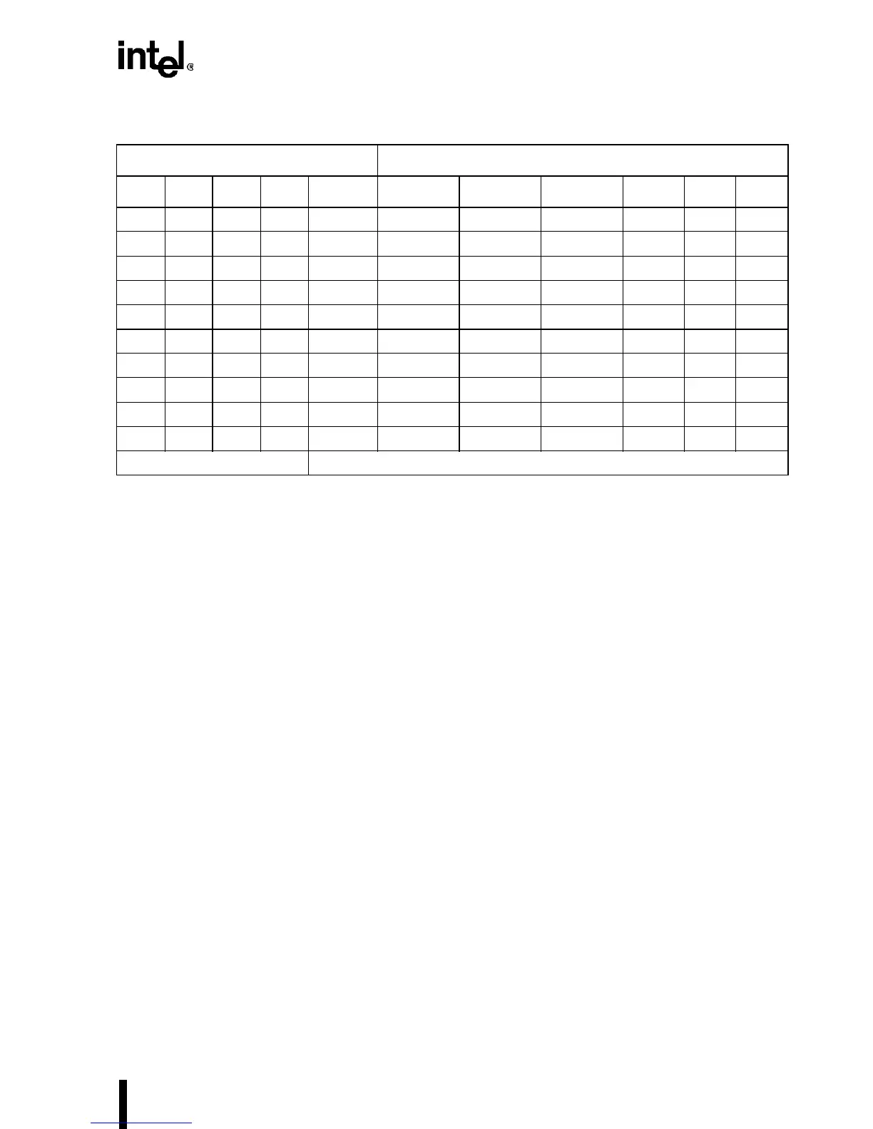
Table 7-9. 32-Bit to 16-Bit Bus Swapping Logic Truth Table (Sheet 2 of 2)
Intel486™ Processor
(3)
8-Bit Interface
(1)
BE3# BE2# BE1# BE0# BEN16# BEN8UH# BEN8UL# BEN8H# BHE#
(2)
A1 A0
Inputs Outputs
NOTES:
1. X implies “do not care” (either 0 or 1).
2. BHE# (byte high enable) is not needed in 8-bit interface.
3.
†
indicates a non-occurring pattern of byte enables; either none are asserted or the pattern has byte
enables asserted for non-contiguous bytes.