10-11
PHYSICAL DESIGN AND SYSTEM DEBUGGING
where e
r
is the relative dielectric constant of the board material and h, w, and t are the dimensions
of the strip. Knowing the line width, the thickness of Cu and the height of dielectric, the charac-
teristic impedance can be easily calculated.
The propagation delay (t
pd
) associated with the trace is a function of the dielectric only. This is
calculated as follows:
t
pd
= 1.017 ns/ft
For G-10 fiberglass epoxy boards (e
r
= 5.0), the propagation delay of micro-strip is calculated to
be 1.77 ns/ft.
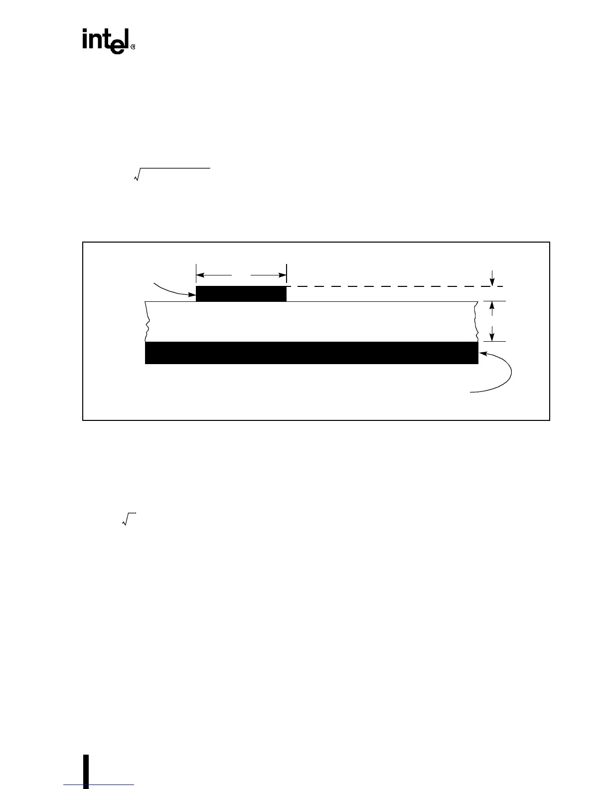
Figure 10-7. Micro-Strip Lines
10.3.1.3 Strip Lines
A strip line is a flat conductor centered in a dielectric medium between two voltage planes. The
characteristic impedance is given theoretically by the equation below:
Z
0
= [60/ ] ln (5.98b/π (0.8w + t)) ohms,
where b = distance between the planes for controlled impedance as shown in Figure 10-8
0.475e
r
0.67+()
w
Micro-strip
h
Dielectric
Ground
Plane
t
e
r