Pin Configuration 124 May 03, 2004
Philips Semiconductors Preliminary User Manual
LPC2119/2129/2194/2292/2294ARM-based Microcontroller
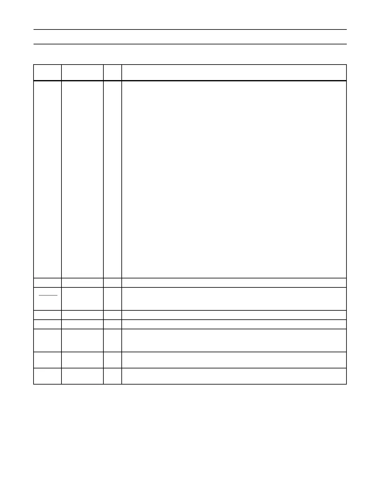
40 I/O
O
P3.23 A23 External memory address line 23.
XCLK Clock output.
36
O P3.24 CS3 Low-active Chip Select 3 signal.
(Bank 3 addresses range 8300 0000 - 83FF FFFF)
35
O P3.25 CS2 Low-active Chip Select 2 signal.
(Bank 2 addresses range 8200 0000 - 82FF FFFF)
30 O
P3.26 CS1 Low-active Chip Select 1 signal.
(Bank 1 addresses range 8100 0000 - 81FF FFFF)
29 O
P3.27 WE Low-active Write enable signal.
28 O
I
P3.28 BLS3 Low-active Byte Lane Select signal (Bank 3).
AIN7 A/D converter, input 7. This analog input is always connected to
its pin.
27 O
I
P3.29 BLS2 Low-active Byte Lane Select signal (Bank 2).
AIN6 A/D converter, input 6. This analog input is always connected to
its pin.
97 O
P3.30 BLS1 Low-active Byte Lane Select signal (Bank 1).
96 O
P3.31 BLS0 Low-active Byte Lane Select signal (Bank 0).
TD1 22 O
TD1:CAN1 transmitter output.Pin is 5 V tolerant with built-in pull-up.
RESET
135 I
External Reset input: A LOW on this pin resets the device, causing I/O ports and
peripherals to take on their default states, and processor execution to begin at address 0.
TTL with hysteresis, 5V tolerant.
XTAL1 142 I Input to the oscillator circuit and internal clock generator circuits.
XTAL2 141 O Output from the oscillator amplifier.
V
SS
3, 9, 26, 38, 54,
67, 79, 93, 103,
107, 111, 128
I Ground: 0V reference.
V
SSA
139 I
Analog Ground: 0V reference. This should nominally be the same voltage as V
SS,
but
should be isolated to minimize noise and error.
V
ssA_PLL
138 I
PLL Analog Ground: 0V reference. This should nominally be the same voltage as V
SS,
but
should be isolated to minimize noise and error.
Table 56: Pin description for LPC2292/2294
Pin
Name
LQFP144
Pin #
Type Description