Introduction 25 May 03, 2004
Philips Semiconductors Preliminary User Manual
LPC2119/2129/2194/2292/2294ARM-based Microcontroller
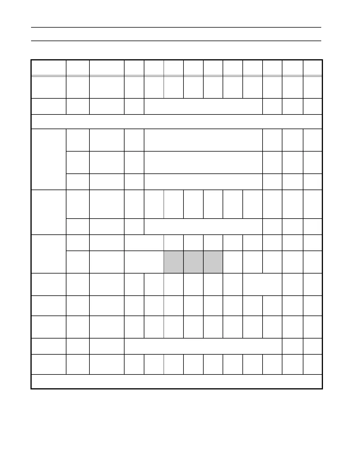
0xE000C014 U0LSR
U0 Line
Status
Register
Rx
FIFO
Error
TEMT THRE BI FE PE OE DR RO 0x60
0xE000C01C U0SCR
U0 Scratch
Pad Register
8 bit data R/W 0
UART1
0xE0010000
U1RBR
(DLAB=0)
U1 Receiver
Buffer
Register
8 bit data RO
un-
defined
U1THR
(DLAB=0)
U1 Transmit
Holding
Register
8 bit data WO NA
U1DLL
(DLAB=1)
U1 Divisor
Latch LSB
8 bit data R/W 0x01
0xE0010004
U1IER
(DLAB=0)
U1 Interrupt
Enable
Register
0000
En.
Mdem
Satus
Int.
En. Rx
Line
Status
Int.
Enable
THRE
Int.
En. Rx
Data
Av.Int.
R/W 0
U1DLM
(DLAB=1)
U1 Divisor
Latch MSB
8 bit data R/W 0
0xE0010008
U1IIR
U1 Interrupt
ID Register
FIFOs Enabled 0 0 IIR3 IIR2 IIR1 IIR0 RO 0x01
U1FCR
U1 FIFO
Control
Register
Rx Trigger
- - -
U0 Tx
FIFO
Reset
U0 Rx
FIFO
Reset
U0
FIFO
Enable
WO 0
0xE001000C U1LCR
U1 Line
Control
Register
DLAB
Set
Break
Stick
Parity
Even
Parity
Select
Parity
Enable
Nm. of
Stop
Bits
Word Length
Select
R/W 0
0xE0010010
U1
MCR
U1 Modem
Control
Register
000
Loop
Back
0 0 RTS DTR R/W 0
0xE0010014 U1LSR
U1 Line
Status
Register
Rx
FIFO
Error
TEMT THRE BI FE PE OE DR RO 0x60
0xE001001C U1SCR
U1 Scratch
Pad Register
8 bit data R/W 0
0xE0010018
U1
MSR
U1 Modem
Status
Register
DCD RI DSR CTS
Delta
DCD
Trailing
Edge
RI
Delta
DSR
Delta
CTS
RO 0
PWM
Table 2: LPC2119/2129/2194/2292/2294 Registers
Address
Offset
Name Description MSB LSB Access
Reset
Value