210
(f) While emulating the H8/36024 group, note that the register specifications at address H’F608 in the actual
device and expansion I/O board (HS36024EIO61H) are different. Table 8.32 lists the specifications and
note on them.
Table 8.33 Register Specifications and Note
Item Register Specifications Note
HS36024EIO61H Bits 4 to 7 (1111): Reserved
Bit 3 (0): Selects the device (0: H8/36024)
Bit 2 (0): Selects whether or not to delete
noise (0: no, 1: yes)
Bit 1 (0): Selects the TXD3 output (0: port, 1:
TXD_3)
Bit 0 (0): Selects whether or not to stop
modules (0: operate, 1: stop)
None
H8/36024 Bits 4 to 7 (1111): Reserved
Bit 3 (1):Reserved (always read as 1 and
writing has no effect)
Bit 2 (1): Reserved (always read as 1 and
writing has no effect)
Bit 1 (0): Selects the TXD3 output (0: port, 1:
TXD_3)
Bit 0 (0): Selects whether or not to stop
modules (0: operate, 1: stop)
For emulation with the
expansion I/O board
(HS36024EIO61H), set
bits 2 and 3 to ‘0’.
Note: The value in parentheses indicates the initial value after a reset.
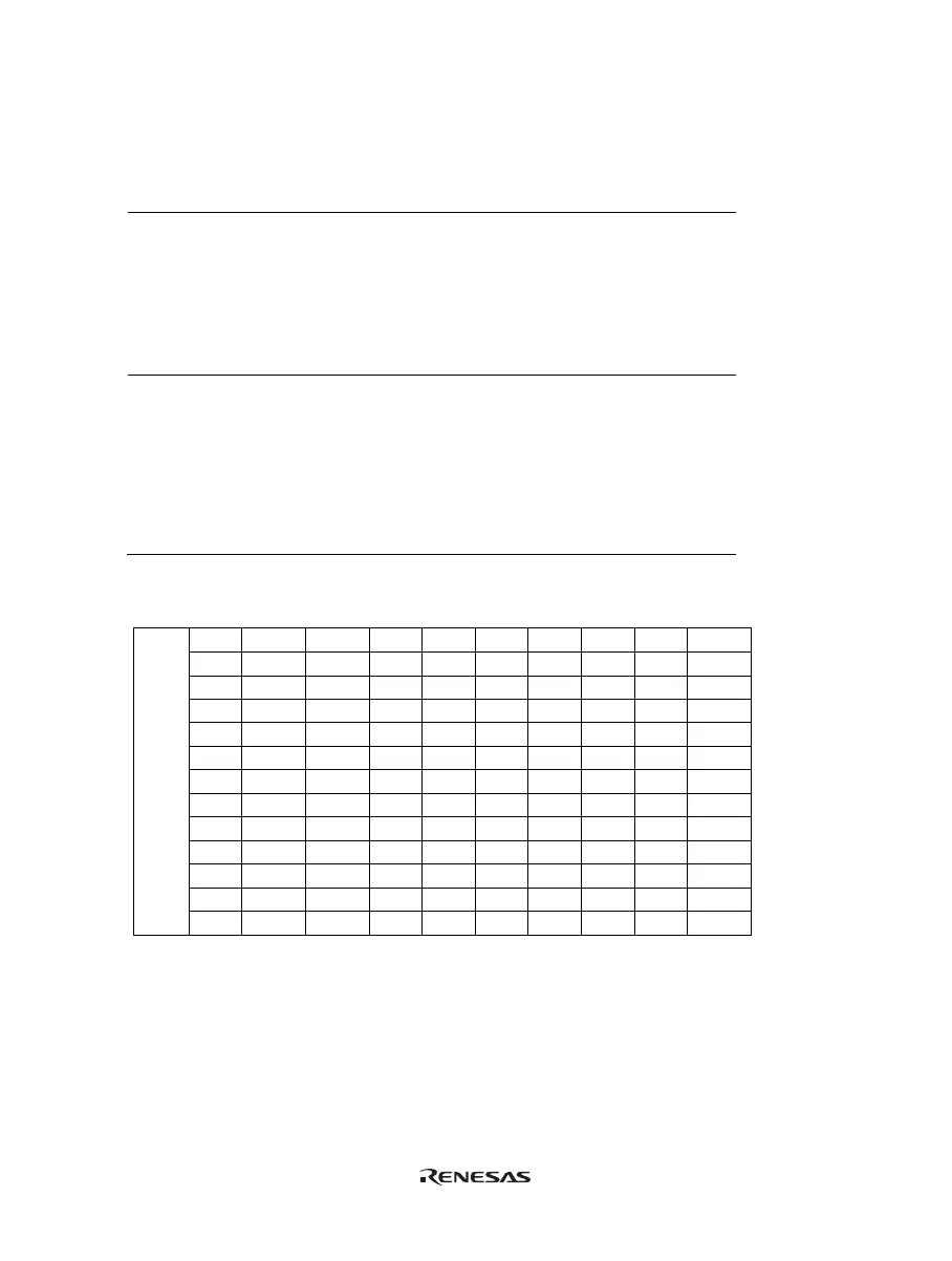
Table 8.34 Differences between the Evaluation Chip and the H8/36014, H8/36024 Registers
Address Register Bit 7 Bit 6 Bit 5 Bit 4 Bit 3 Bit 2 Bit 1 Bit 0
H'F730 ⎯ ⎯ ⎯ ⎯ ⎯ ⎯ ⎯ ⎯ ⎯
H'F731 ⎯ ⎯ ⎯ ⎯ ⎯ ⎯ ⎯ ⎯ ⎯
H'FFE0 PMR1 IRQ3 IRQ2 IRQ1 IRQ0 TXD2 PWM TXD TMOW
H'FFE1 PMR5 POF57 POF56 WKP5 WKP4 WKP3 WKP2 WKP1 WKP0
H'FFE2 PMR3 POF27 POF26 POF25 POF24 POF23 ⎯ ⎯ ⎯
H'FFF1 SYSCR2 SMSEL LSON DTON MA2 MA1 MA0 SA1 SA0
H'FFF2 IEGR1 NMIEG ⎯ ⎯ ⎯ IEG3 IEG2 IEG1 IEG0
H'FFF4 IENR1 IENDT IENTA IENWP ⎯ IEN3 IEN2 IEN1 IEN0
H'FFF5 IENR2 IENTB3 IENTB2 IENTB1 ⎯ ⎯ ⎯ ⎯ ⎯
H'FFF9 MSTCR1 MSTS4 MSTIIC MSTS3 MSTAD MSTWD MSTTW MSTTV MSTTA
H'FFFA MSTCR2 MSTS3_2 MSTTB3 MSTTB2 MSTTB1 MSTTX ⎯ MSTTZ0 MSTPWM
H8/3660
(Evalua-
tion chip)
H'FFFB MSTCR3 ⎯ ⎯ ⎯ ⎯ ⎯ ⎯ ⎯ MSTS4_2
 Loading...


