215
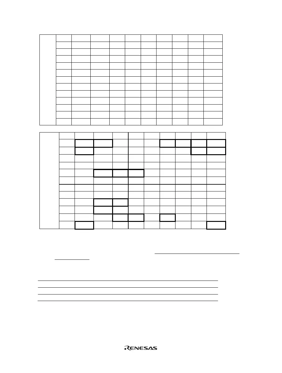
Table 8.43 Differences between the Evaluation Chip and the H8/36049 Registers
Address Register Bit 7 Bit 6 Bit 5 Bit 4 Bit 3 Bit 2 Bit 1 Bit 0
H'F730 ⎯ ⎯ ⎯ ⎯ ⎯ ⎯ ⎯ ⎯ ⎯
H'F731 ⎯ ⎯ ⎯ ⎯ ⎯ ⎯ ⎯ ⎯ ⎯
H'FFE0 PMR1 IRQ3 IRQ2 IRQ1 IRQ0 TXD2 PWM TXD TMOW
H'FFE1 PMR5 POF57 POF56 WKP5 WKP4 WKP3 WKP2 WKP1 WKP0
H'FFE2 PMR3 POF27 POF26 POF25 POF24 POF23 ⎯ ⎯ ⎯
H'FFF1 SYSCR2 SMSEL LSON DTON MA2 MA1 MA0 SA1 SA0
H'FFF2 IEGR1 NMIEG ⎯ ⎯ ⎯ IEG3 IEG2 IEG1 IEG0
H'FFF4 IENR1 IENDT IENTA IENWP ⎯ IEN3 IEN2 IEN1 IEN0
H'FFF5 IENR2 IENTB3 IENTB2 IENTB1 ⎯ ⎯ ⎯ ⎯ ⎯
H'FFF9 MSTCR1 MSTS4 MSTIIC MSTS3 MSTAD MSTWD MSTTW MSTTV MSTTA
H'FFFA MSTCR2 MSTS3_2 MSTTB3 MSTTB2 MSTTB1 MSTTX ⎯ MSTTZ0 MSTPWM
H8/3660
(Evalua-
tion chip)
H'FFFB MSTCR3 ⎯ ⎯ ⎯ ⎯ ⎯ ⎯ ⎯ MSTS4_2
Address Register Bit 7 Bit 6 Bit 5 Bit 4 Bit 3 Bit 2 Bit 1 Bit 0
H'F730 LVDCR LVDE ⎯ ⎯ ⎯ LVDSEL LVDRE LVDDE LVDUE
H'F731 LVDSR ⎯ ⎯ ⎯ ⎯ ⎯ ⎯ LVDDF LVDUF
H'FFE0 PMR1 IRQ3 IRQ2 IRQ1 IRQ0 TXD2 PWM TXD TMOW
H'FFE1 PMR5 POF57 POF56 WKP5 WKP4 WKP3 WKP2 WKP1 WKP0
H'FFE2 PMR3 ⎯ ⎯ ⎯ POF24 POF23 ⎯ ⎯ ⎯
H'FFF1 SYSCR2 SMSEL LSON DTON MA2 MA1 MA0 SA1 SA0
H'FFF2 IEGR1 NMIEG ⎯ ⎯ ⎯ IEG3 IEG2 IEG1 IEG0
H'FFF4 IENR1 IENDT IENTA IENWP ⎯ IEN3 IEN2 IEN1 IEN0
H'FFF5 IENR2 ⎯ ⎯ IENTB1 ⎯ ⎯ ⎯ ⎯ ⎯
H'FFF9 MSTCR1 ⎯ MSTIIC MSTS3 MSTAD MSTWD MSTTW MSTTV MSTTA
H'FFFA MSTCR2 MSTS3_2 ⎯ ⎯ MSTTB1 ⎯ ⎯ MSTTZ MSTPWM
H8/36049
H'FFFB ⎯ ⎯ ⎯ ⎯ ⎯ ⎯ ⎯ ⎯ ⎯
(8) Warnings that Apply to H8/36109 Group Programming
(a) The description given in the hardware manual is “Initial value: 0. Reserved. These bits are always read as
0”. However, the description in the emulator manual is “Always specify 0. These bits are always read as
the specified values”.
Table 8.44 Differences between the H8/36109 Group Products (1)
Target Address Register Name Bits
H'FFF5 Interrupt enable register 2 7 and 6
H'FFF9 Module standby control register 1 7, 4, and 2
H'FFFA Module standby control register 2 6, 5, 3, and 1
 Loading...


