RL78/F13, F14 CHAPTER 3 CPU ARCHITECTURE
R01UH0368EJ0210 Rev.2.10 89
Dec 10, 2015
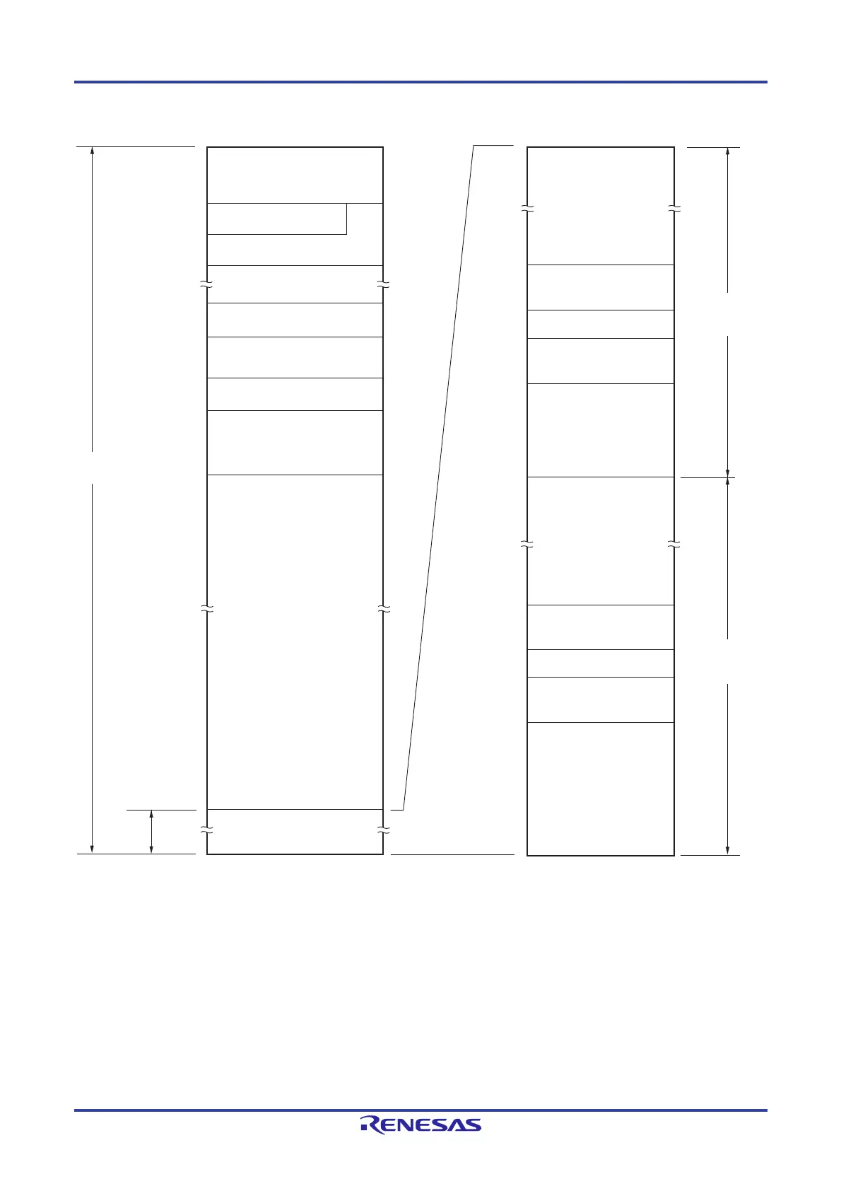
Figure 3-1. Memory Map (R5F10AmA (m = 6, A, B, G))
Notes 1. Do not allocate RAM addresses which are used as stack area, data buffers used by the libraries, branch
destinations for vectored interrupt servicing, or DTC transfer destinations/transfer sources to the area FFE20H
to FFEDFH when performing self-programming and rewriting the data flash memory.
2. Instructions can be executed from the RAM area excluding the general-purpose register area.
3. When boot swap is not used: Set the option bytes to 000C0H to 000C3H, and the on-chip debug security IDs
to 000C4H to 000CDH.
When boot swap is used: Set the option bytes to 000C0H to 000C3H and 020C0H to 020C3H, and the on-
chip debug security IDs to 000C4H to 000CDH and 020C4H to 020CDH.
4. Writing boot cluster 0 can be prohibited depending on the setting of security (see 30.6 Security Settings).
Caution When executing instructions from the RAM area, be sure to initialize the used RAM area + 10 bytes
with any desired value.
FFFFFH
00000H
FFF00H
FFEFFH
FFEE0H
FFEDFH
F0800H
F07FFH
F0000H
EFFFFH
04000H
03FFFH
FFB00H
FF
AFFH
F2000H
F1FFFH
F1000H
F0FFFH
03FFFH
00080H
0007FH
00000H
000C0H
000BFH
02000H
01FFFH
000C4H
000C3H
02080H
0207FH
020C0H
020BFH
020C4H
020C3H
03FFFH
000CEH
000CDH
020CEH
020CDH
F4000H
F3FFFH
Reserved
Reserved
Reserved
Special function register (SFR)
256 bytes
General-purpose register
32 bytes
RAM
Notes 1, 2
1 KB
Special function register (2nd SFR)
2 KB
Code flash memory
16 KB
Data memory
space
Program
memory
space
Data flash memory
4 KB
Vector table area
128 bytes
CALLT table area
64 bytes
Program area
Option byte area
Note 3
4 bytes
Vector table area
128 bytes
CALLT table area
64 bytes
Option byte area
Note 3
4 bytes
Program area
On-chip debug security
ID setting area
Note 3
10 bytes
Boot cluster 0
Note 4
Boot cluster 1
On-chip debug security
ID setting area
Note 3
10 bytes
Mirror
8 KB
 Loading...


