RL78/F13, F14 CHAPTER 6 TIMER ARRAY UNIT
R01UH0368EJ0210 Rev.2.10 466
Dec 10, 2015
6.3.17 PWM output delay control register 1 (PWMDLY1)
This register controls output delay of PWM output signal output from the TO0n pin.
Set the PWMDLY1 register by a 16-bit memory manipulation instruction.
Reset signal generation clears this register to 0000H.
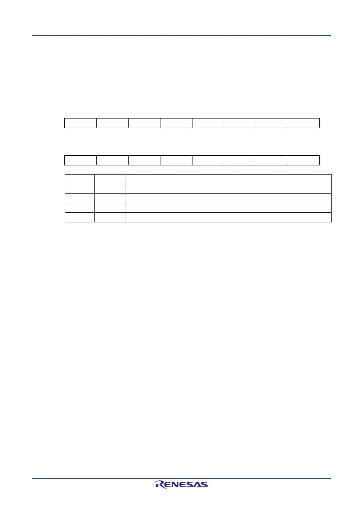
Address: F022BH After reset: 00H R/W
Symbol 15 14 13 12 11 10 9 8
PWMDLY1 TO071 TO070 TO061 TO060 TO051 TO050 TO041 TO040
Address: F022AH After reset: 00H R/W
Symbol 7 6 5 4 3 2 1 0
PWMDLY1 TO031
Note
TO030
Note
TO021
Note
TO020
Note
TO011 TO010 0 0
TO0n1 TO0n0 PWM output delay control of timer array unit 0 TO0n
0 0 No delay
0 1 Delayed by one cycle of the CPU/peripheral hardware clock (fCLK).
1 0 Delayed by two cycles of the CPU/peripheral hardware clock (fCLK).
1 1 Delayed by three cycles of the CPU/peripheral hardware clock (fCLK).
Note If this register is set for a delay, this affects PWM output of TO0n, but doesn’t affect the operation of the
timer output signal to peripheral functions.
Remark n: Channel number (n = 1 to 7)
Cautions 1. Set this register before outputting a PWM output signal (do not change the setting during
operation).
2. Set this register with a 16-bit memory manipulation instruction. Do not set this register with a
1-bit or 8-bit memory manipulation instruction.
3. If this register is not used for PWM output, it should be cleared to 0. This is because the timer
output is delayed.
4. When setting this register after the PWM output is stopped, wait for four cycles of the
CPU/peripheral hardware clock (f
CLK) before the setting.
5. Even if this register is set for a delay, this doesn’t affect the operation of other pin functions
multiplexed on the same pin as the TO0n pin function (n = 1 to 7).
 Loading...


