RL78/F13, F14 CHAPTER 5 CLOCK GENERATOR
R01UH0368EJ0210 Rev.2.10 389
Dec 10, 2015
5.3.11 LIN Clock Select Register (LINCKSEL)
This register is used to control the communication clock source supplied to the LIN.
Set the LINCKSEL register by a 1-bit or 8-bit memory manipulation instruction.
Writing to the LINCKSEL register is disabled when the GCSC bit of the IAWCTL register is set to 1.
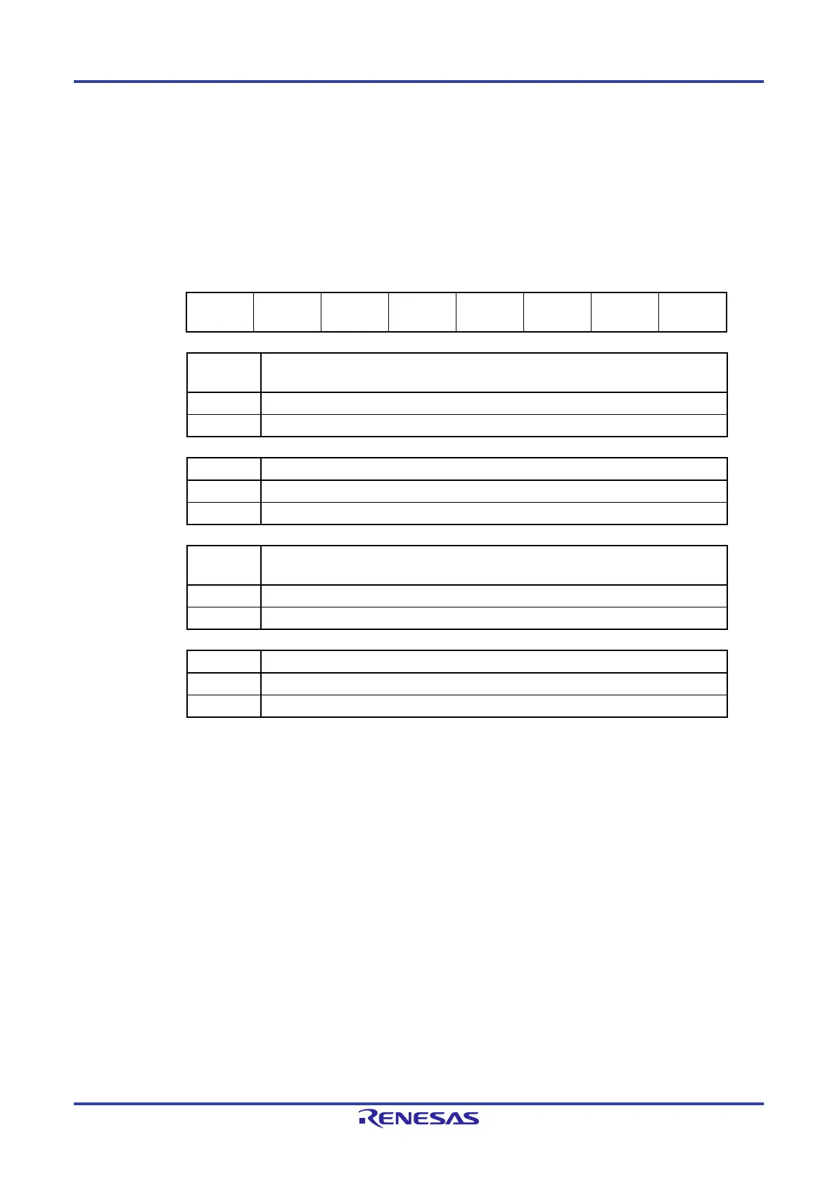
Figure 5-18. Format of LIN Clock Select Register (LINCKSEL)
Address: F02C3H After reset: 00H R/W
Symbol 7 6 <5> <4> 3 2 <1> <0>
LINCKSEL 0 0
LIN1MCKE
Note
LIN0MCKE
0 0
LIN1MCK
Note
LIN0MCK
LIN1MCKE
Note
Control of supplying or stopping LIN1 communication clock source
0 Stops LIN communication clock source supply.
1 Enables LIN communication clock source supply.
LIN0MCKE Control of supplying or stopping LIN0 communication clock source
0 Stops LIN communication clock source supply.
1 Enables LIN communication clock source supply.
LIN1MCK
Note
Control of selecting LIN1 communication clock source
0 Selects the f
CLK
clock.
1 Selects the f
MX
clock.
LIN0MCK Control of selecting LIN0 communication clock source
0 Selects the f
CLK
clock.
1 Selects the f
MX
clock.
Note Only in the RL78/F14 products with 48 pins and at least 128 Kbytes of code flash memory and
the 100-pin products of the RL78/F14.
Cautions 1. Select the LINn operating clock with the LINnMCK bit before setting the LINnMCKE
(n = 0, 1) bit to 1.
2. When operating LINn in SNOOZE mode, set the LINnMCK bit to 0.
3. In case of LINnMCK is set to 1, do not use the timeout error detection.
In that case, set at least 1.2 times the frequency of the LIN communication clock
source to the f
CLK clock.
<R>
 Loading...


