RL78/F13, F14 CHAPTER 6 TIMER ARRAY UNIT
R01UH0368EJ0210 Rev.2.10 440
Dec 10, 2015
6.3.1 Peripheral enable register 0 (PER0)
This registers is used to enable or disable supplying the clock to the peripheral hardware. Clock supply to a hardware
macro that is not used is stopped in order to reduce the power consumption and noise.
When the timer array unit 0 is used, be sure to set bit 0 (TAU0EN) of this register to 1.
When the timer array unit 1 is used, be sure to set bit 1 (TAU1EN) of this register to 1.
Set the PER0 register by a 1-bit or 8-bit memory manipulation instruction.
Reset signal generation clears this register to 00H.
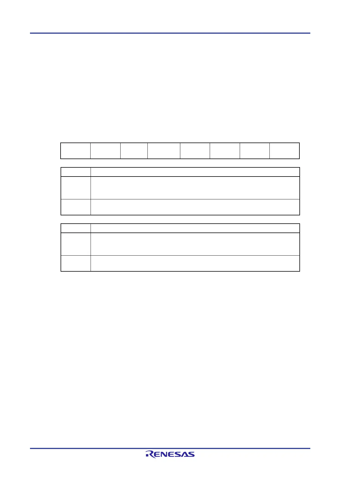
Figure 6-10. Format of Peripheral Enable Register 0 (PER0)
Address: F00F0H After reset: 00H R/W
Symbol <7> 6 <5> <4> <3> <2> <1> <0>
PER0 RTCEN 0
ADCEN
IICA0EN
Notes1,
2
SAU1EN
Note1
SAU0EN
TAU1EN
Note1
TAU0EN
TAU1EN Control of timer array unit 1 input clock
0
Stops supply of input clock.
SFR used by the timer array unit 1 cannot be written.
The timer array unit 1 is in the reset status.
1
Supplies input clock.
SFR used by the timer array unit 1 can be read/written.
TAU0EN Control of timer array 0 unit input clock
0
Stops supply of input clock.
SFR used by the timer array unit 0 cannot be written.
The timer array unit 0 is in the reset status.
1
Supplies input clock.
SFR used by the timer array unit 0 can be read/written.
Notes 1. Not provided in RL78/F13 (LIN incorporated) products with 20, 30, 32, 48, or 64 pins and 16 Kbytes
to 64 Kbytes of code flash memory.
2. Not provided in RL78/F13 (CAN and LIN incorporated) with 30 pins and RL78/F14 with 30 pins.
Cautions 1. When setting the timer array unit, be sure to set the TAUmEN bit to 1 first. If TAUmEN =
0, writing to a control register of timer array unit is ignored, and all read values are default
values (except for the timer input select registers 0, 1, 2 (TIS0, TIS1, TIS2), noise filter
enable registers 1, 2 (NFEN1, NFEN2), port mode registers 1, 3, 4, 7, 12 (PM1, PM3, PM4,
PM7, PM12), port registers 1, 3, 4, 7, 12 (P1, P3, P4, P7, P12), and PWM output delay control
registers 1, 2 (PWMDLY1, PWMDLY2)).
2. Be sure to clear the following bits to 0.
Bits 1, 3, 4, and 6 in RL78/F13 (LIN incorporated) products with 20, 30, 32, 48, or 64 pins
and 16 Kbytes to 64 Kbytes of code flash memory
Bits 4 and 6 in the RL78/F13 (CAN and LIN incorporated) products with 30 pins, or in the
RL78/F14 products with 30 pins
Bit 6 in the products other than above
 Loading...


