RL78/F13, F14 CHAPTER 5 CLOCK GENERATOR
R01UH0368EJ0210 Rev.2.10 372
Dec 10, 2015
5.3.2 System Clock Control Register (CKC)
This register is used to select a CPU/peripheral hardware clock and a main system clock.
Set the CKC register by a 1-bit or 8-bit memory manipulation instruction.
Writing to the CKC register is disabled when the GCSC bit of the IAWCTL register is set to 1.
Reset signal generation sets this register to 00H.
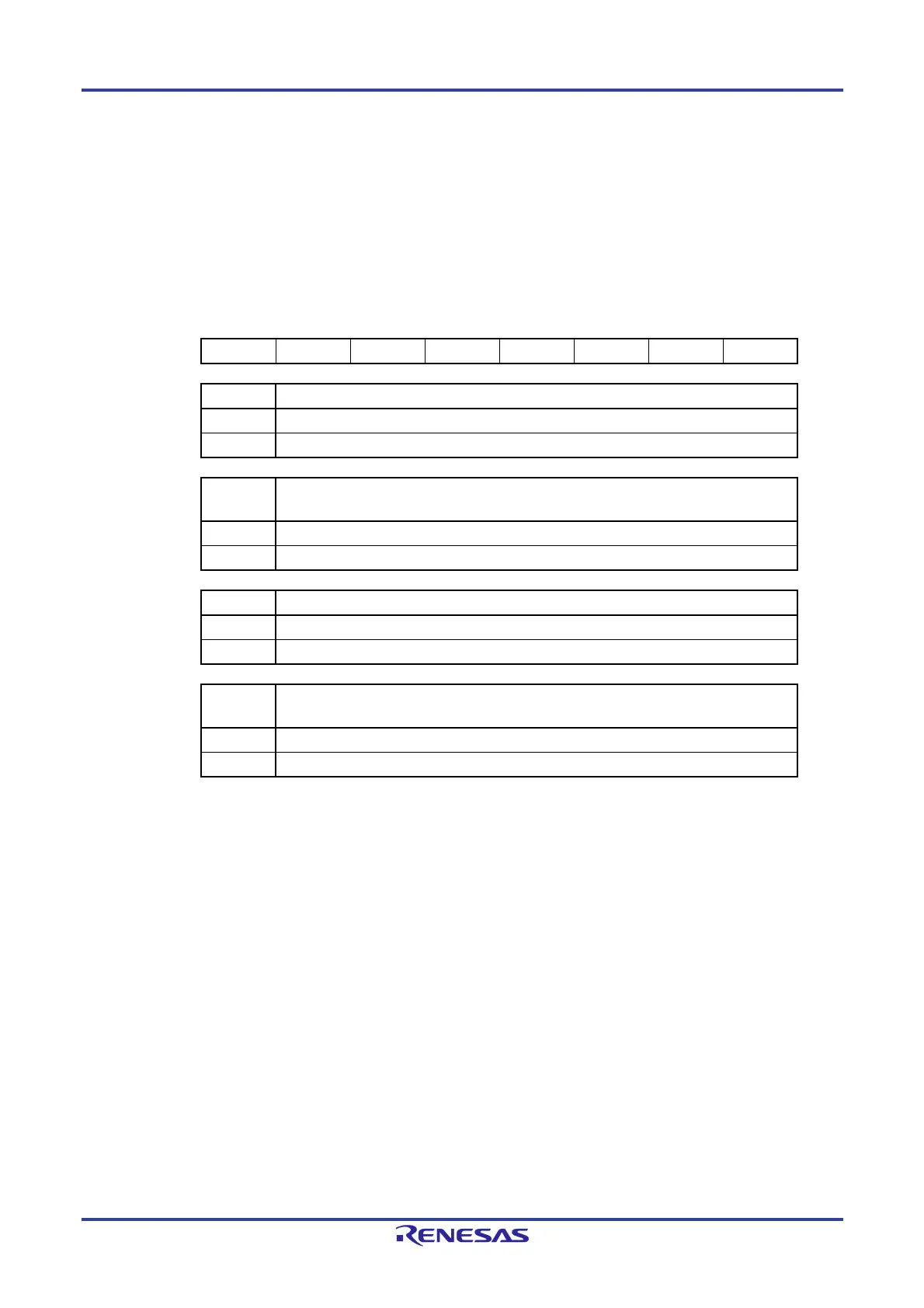
Figure 5-4. Format of System Clock Control Register (CKC)
Address: FFFA4H After reset: 00H R/W
Note 1
Symbol <7> <6> <5> <4> 3 2 1 0
CKC CLS CSS MCS MCM0 0 0 0 0
CLS Status of CPU/peripheral hardware clock (fCLK)
0 Main system/PLL select clock (fMP)
1 Subsystem/low-speed on-chip oscillator select clock (fSL)
CSS
Notes 2, 3
Selection of CPU/peripheral hardware clock (fCLK)
0 Main system/PLL select clock (fMP)
1 Subsystem/low-speed on-chip oscillator select clock (fSL)
MCS Status of main system clock (fMAIN)
0 High-speed on-chip oscillator clock (fIH)
1 High-speed system clock (fMX)
MCM0
Notes 2, 4, 5
Main system clock (f
MAIN) operation control
0 Selects the high-speed on-chip oscillator clock (fIH) as the main system clock (fMAIN)
1 Selects the high-speed system clock (fMX) as the main system clock (fMAIN)
Notes 1. Bits 7 and 5 are read-only.
2. Changing the value of the MCM0 bit is prohibited while the CSS bit is set to 1.
3. When setting the CSS bit in the 20-, 30-, or 32-pin products, set bit 0 (SELLOSC) in the clock
select register (CKSEL) to 1 (Selects f
IL).
4. Changing the value of the MCM0 bit is prohibited while the PLLON bit is set to 1.
5. To change the MCM0 bit from 0 to 1 while FRQSEL4 = 1 in the corresponding user option
byte (at 000C2H or 020C2H), stop counting by the timer RD (setting the TSTART0 and
TSTART1 bits in the TRDSTR register to 0) and disable clock or buzzer output (by setting the
PCLOE0 bit in the CKS0 register to 0) before changing the MCM0 bit.
 Loading...


