RL78/F13, F14 CHAPTER 23 STANDBY FUNCTION
R01UH0368EJ0210 Rev.2.10 1540
Dec 10, 2015
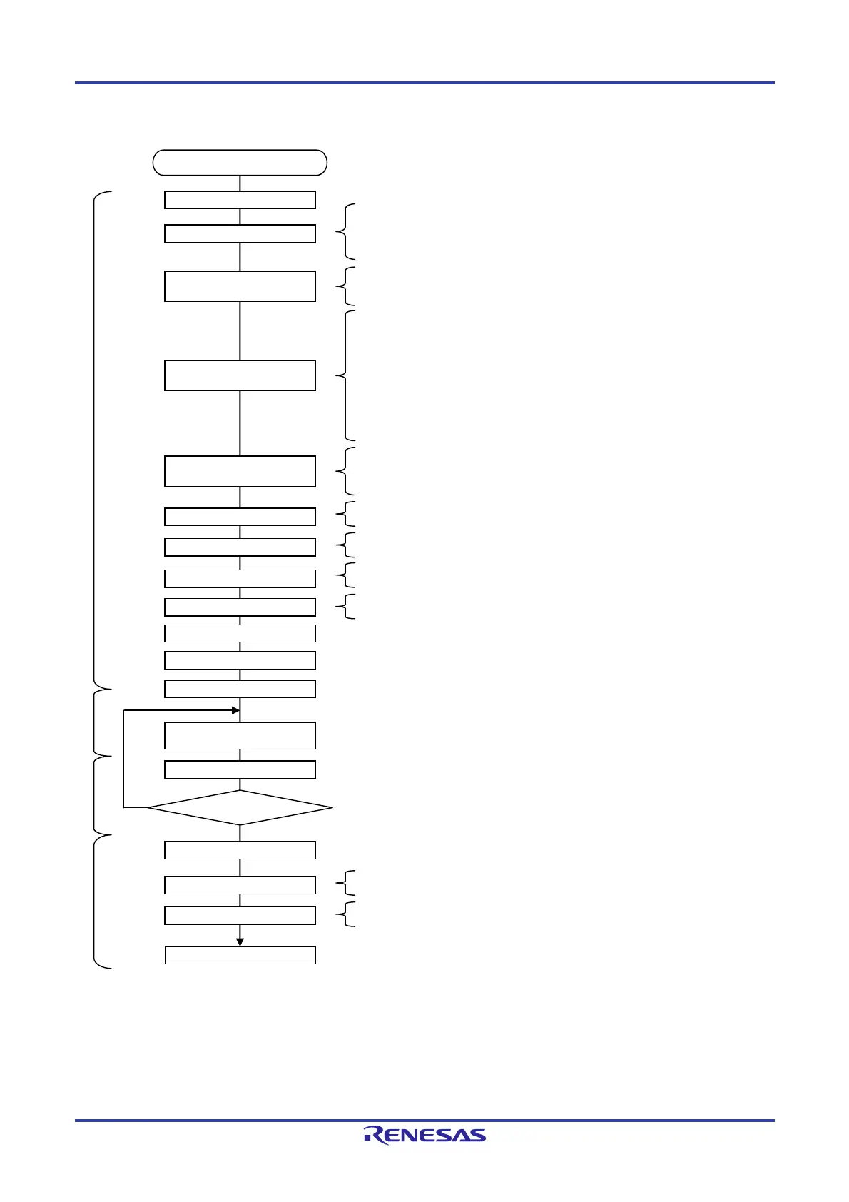
Figure 23-10. Example of Settings for SNOOZE Mode Status Output
Note 1. On the transition from STOP (or SNOOZE) mode to normal operation, stop A/D converter operations
and then stop counting by timer RD0 (after changing the CPU clock to f
SL) as shown in the figure above.
Caution For details on the settings of registers for the A/D converter, timer RD, port functions, etc., see
the corresponding chapters.
Return to normal operation.
Yes
No
To user processing
Example of setting
SNOOZE mode status output
Disable interrupts (DI).
Stop counting by timer RD0.
Note 1
Stop A/D converter operations.
Note 1
INTAD generated?
Execute A/D conversion.
Use timer RD0 to generate
a hardware trigger.
Enter STOP mode.
Enable interrupts (EI).
Set a clock (f
CLK = fIH).
Start counting by timer RD0.
Set a clock (f
CLK = fSL).
Enable A/D converter operations.
Set A/D and timer RD interrupts.
Set the target port pin as a
SNOOZE mode status output pin.
Initialize the timer
RD-related registers.
Normal operation
STOPSNOOZE
Normal operation
Set the ELC or A/D converter
trigger select 0 control circuit.
Initialize the A/D-related registers.
• PER0.ADCEN = 1.
• Use the ADPC, PMCx, PMx registers to set the A/D pins as analog input pins.
• Set the ADM0, ADM2, ADUL/ADLL, ADS registers.
• ADM1 = 0xE1 (selecting hardware trigger wait mode, one-shot conversion mode,
and the hardware trigger signal selected by the ELC module or ADTRGS0 register).
Enable generation of the timer RD0 compare match B interrupt request as
the trigger for A/D conversion.
• RL78/F14: ELSELR09.ELSELR09[3:0] = 0001b.
• RL78/F13: ADTRGS0.ADTRGS00 = 1.
• PER1.TRD0EN = 1.
• TRDSTR.CSEL0 = 1 (continuing counting after compare match with the TRDGRA0 register).
• TRDPMR.TRDPWMB0 = 1 (selecting the PWM function of the TRDIOB0 pin).
• TRDPMR.TRDPWMC0 = 1 (selecting the PWM function of the TRDIOC0 pin).
• TRDOER1.EC0 = 0 (enabling TRDIOC0 output).
• TRDOCR.TOC0 = 0 (setting the low level as TRDIOC0 initial output).
• TRDCR0.CCLR[2:0] = 001b (clearing on compare match with the TRDGRA0 register).
• TRDPOCR0.POLC = 0 (setting the TRDIOC0 output signal as active low).
• Set the TRDGRA0 register (SNOOZE status output interval).
• Set the TRDGRB0 register (A/D converter start wait time).
• Set the TRDGRC0 register (A/D converter start wait time + A/D conversion time).
• Set the bit for the pin selected as an SNZOUT pin in the port mode register to 0 (output mode).
• Set the bit for the SNZOUT pin in the port register to 0 (output of the low level).
• Set the PSNZCNTn.SNZACT[7:0] bits (selecting the active level).
• Set the PSNZCNTn.OUTEN[7:0] bits (enabling output).
• MK1H.ADMK = 0 (enabling processing of the A/D interrupt).
• MK0H.TRDMK0 = 1 (disabling processing of the timer RD0 interrupt).
• ADM2.AWC = 1 (using the SNOOZE mode function).
• ADM0.ADCE = 1 (enabling A/D converter operation).
• OSMC.RTCLPC = 0 (enabling supply of the f
SL clock to peripheral functions).
• CKC.CSS = 1, CKC.CLS = 1 (selecting f
SL as the CPU clock).
• CKSEL.TRD_CKSEL = 1 (selecting f
SL as the timer RD clock).
• TRDSTR.TSTART0 = 1 (starting counting by timer RD0).
CKC.CSS = 0, CKC.CLS = 0 (selecting f
IH as the CPU clock).
When no interrupt processing is to be used in recovery, disable interrupts (DI).
Use timer RD0 to generate a SNOOZE mode status output and A/D trigger (internal signal).
Enter SNOOZE mode.
Start A/D conversion in SNOOZE mode.
Generation of an A/D conversion end interrupt (INTAD) is controlled by the settings of the ADM2.
ADRCK bit, and of the ADUL and ADLL registers. The result of A/D conversion is stored in the
ADCR or ADCRH register. If no INTAD has been generated, this microcontroller will return to the
STOP mode. The ADCR or ADCRH register will not hold a result of conversion.
If interrupts are enabled, the interrupt processing will proceed. If interrupts are disabled,
the instruction following the STOP instruction will be executed.
• ADM0.ADCE = 0 (stopping A/D converter operations).
• ADM2.AWC = 0 (the SNOOZE mode function is not in use).
• CKC.CSS = 1, CKC.CLS = 1 (selecting f
SL as the CPU clock).
• TRDSTR.TSTART0 = 0 (stopping counting by timer RD0).
 Loading...


