RL78/F13, F14 CHAPTER 8 TIMER RD
R01UH0368EJ0210 Rev.2.10 615
Dec 10, 2015
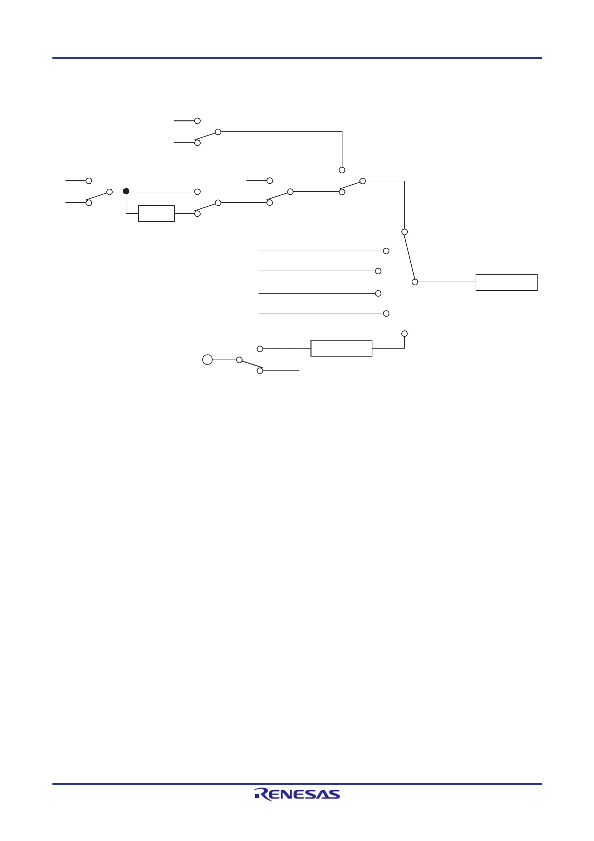
Figure 8-40. Count Source Block Diagram
Notes 1. f
IH cannot be selected when it is 64 MHz or 48 MHz. fPLL can be selected when it is over 32 MHz.
2. With this setting, select fCLK as the timer RD operating clock (fTRD).
Remark i = 0 or 1
TCK0 to TCK2, CKEG0, CKEG1: Bits in TRDCRi register
STCLK: Bit in TRDFCR register
FREQSEL4: Bit in user option byte (000C2H/020C2H)
MCM0: Bit in CKC register
SELPLL: Bit in PLLCTL register
PLLDIV1: Bit in PLLCTL register
SELPLLS: Bit in PLLSTS register
SELLOSC: Bit in CKSEL register
TDC_CKSEL: Bit in CKSEL register
Set the pulse width of the external clock applied to the TRDCLK0 pin to three or more cycles of the timer RD operating
clock (f
TRD).
f
S
f
TRD
UB
SELLOSC = 0
f
IL
TCK2
to
TCK0
Count source
TRDIOA0
TRD_CKSEL = 0
f
IH
f
SL
MCM0 = 0
f
MX
f
MAIN
PLL
SELPLL = 1
f
PLL
f
MP
f
CLK
FRQSEL4 = 0
and (PLLDIV1 = 0
or SELPLLS = 0)
SELPLL = 0
MCM0 =
1
FRQSEL4 = 1
or (PLLDIV1 = 1
and SELPLLS = 1)
TRD_CKSEL = 1
TRDi
f/8
f
/32
f/4
f
TRD
TRD
TRD
TRD
/2
=100B
=011B
=010B
=001B
=000B
=101
B
CKEG0, CKEG1
STCLK = 1
STCLK =
0
TRDIOA0 I/O or I/O port
SELLOSC = 1
PLLPLL
TRDi
TRDi register
Active edge
selection
TRDCLK0/
Note 1
Note 2
Note 2
Note 2
Note 2
 Loading...


