RL78/F13, F14 CHAPTER 15 SERIAL ARRAY UNIT
R01UH0368EJ0210 Rev.2.10 799
Dec 10, 2015
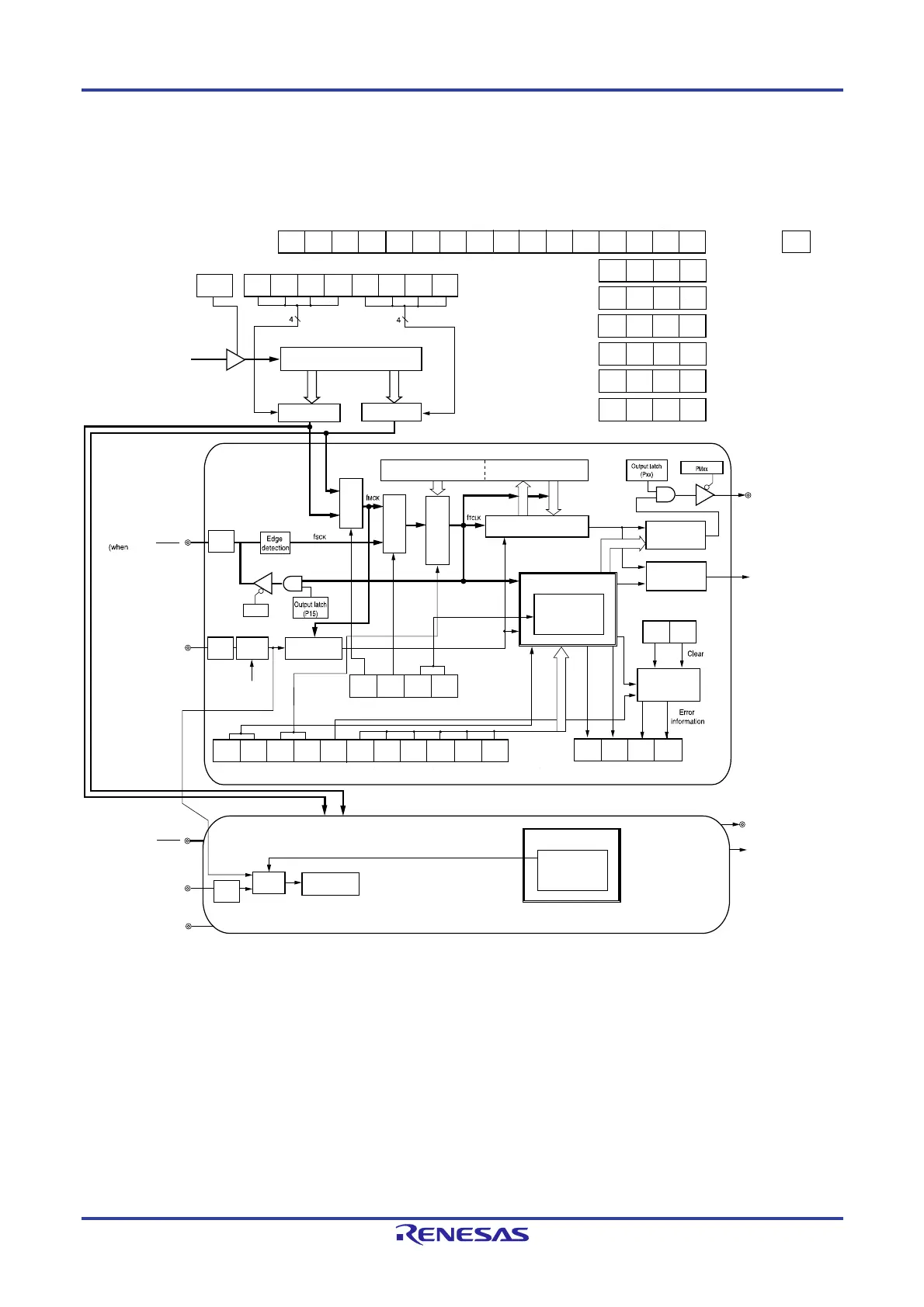
Figure 15-2 shows the block diagram of the serial array unit 1.
Figure 15-2. Block Diagram of Serial Array Unit 1
Caution: If operation is stopped (SEmn = 0), the upper 7 bits set the clock division, and the lower bits have
no meaning.
If operation is in progress (SEmn = 1), the serial data register 10 functions as the buffer register.
Serial clock select register 1 (SPS1)
PRS
113
PRS
103
PRS
112
PRS
111
PRS
110
PRS
102
PRS
101
PRS
100
f
CLK
f
CLK
/2
0
to f
CLK
/2
11
Selector
f
CLK
/2
0
to
f
CLK
/2
11
Selector
CKS10
MD101CCS10
MD102
Mode selection
CSI20 or IIC20
or UART2
(for transmission)
Communication controller
Shift register
Serial data register 10 (SDR10)
Note
Interrupt
controller
SAU1EN
Peripheral enable
register 0 (PER0)
Serial data output pin
(when CSI10: SO10)
(when IIC10: SDA10)
(when UART1: TxD1)
Serial mode register 10 (SMR10)
(Buffer register block)
(Clock division setting block)
Error controller
TXE
10
RXE
10
DAP
10
CKP
10
Serial communication operation setting register 10 (SCR10)
0
PECT
10
Serial flag clear trigger
register 10 (SIR10)
OVCT
10
PTC
101
DLS
101
PTC
100
DIR
10
SLC
101
DLS
100
TSF
10
OVF
10
BFF
10
PEF
10
Serial status register 10 (SSR10)
Output
controller
Serial transfer end interru
(when CSI10: INTCSI10)
(when IIC10: INTIIC10)
(when UART1: INTST1)
Channel 0
CK11
CK10
Communication controller
CK11
CK10
Serial clock I/O pin
CSI10: SCK10)
(when IIC10: SCL10)
PM15
Edge/level
detection
Serial data input pin
(when CSI10: SI10)
(when IIC10: SDA10)
(when UART1: RxD1)
Noise
elimination
enabled/
disabled
SNFEN20
Noise filter enable
register 0 (NFEN0)
SNFEN
10
When UART1
SOE10
Serial output
enable register 1
(SOE1)
SE11 SE10
Serial channel
enable status
register 1 (SE1)
ST11 ST10
Serial channel
stop register 1
(ST1)
SS11 SS10
Serial channel
start register 1
(SS1)
SOL11
SOL10
SOE11
Serial output
level register 1
(SOL1)
Selector
Clock controller
Selector
Communication
status
Prescaler
Serial output register 1 (SO1)
CKO10CKO11
SO11
SO10
0
0
00
0
0
00
Synchro-
nous
circuit
Synchro-
nous
circuit
Channel 1
Serial data input pin
(when CSI11: SI11)
(when IIC11: SDA11)
Serial clock I/O pin
(when CSI11: SCK11)
(when IIC11: SCL11)
Selector
Synchro-
nous
circuit
Edge/level
detection
Mode selection
CSI11 or IIC11
or UART1
(for reception)
Serial transfer end interru
(when CSI11: INTCSI11)
(when IIC11: INTIIC11)
(when UART1: INTSR1)
Serial data output pin
(when CSI11: SO11)
(when IIC11: SDA11)
0
00
00
00
0
0
0
0
00
SSE11
SSE10
Serial slave
select enable
register 1 (SSE1)
0
0
Slave select input pin
(when CSI11: SSI11)
 Loading...


