RL78/F13, F14 CHAPTER 29 OPTION BYTE
R01UH0368EJ0210 Rev.2.10 1618
Dec 10, 2015
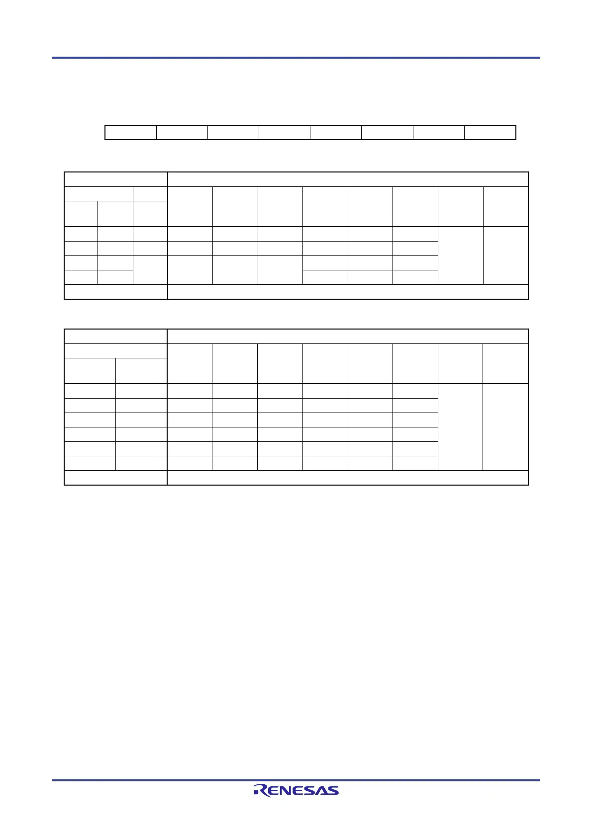
Figure 29-2. Format of User Option Byte (000C1H/020C1H) (1/2)
Address: 000C1H/020C1H
Note 1
After reset: (user setting value
Note 2
)
7 6 5 4 3 2 1 0
VPOC2 VPOC1 VPOC0 CLKMB LVIS1 LVIS0 LVIMDS1 LVIMDS0
LVD setting (interrupt & reset mode)
Detection voltage Option byte Setting Value
VLVDH VLVDL VPOC2
VPOC1
VPOC0 CLKMB LVIS1 LVIS0 LVIMDS1 LVIMDS0
Rising
edge
Falling
edge
Falling
edge
4.42 V 4.32 V 2.75 V 0 0 1
Note 3
0 0 1 0
4.62 V 4.52 V 2.75 V 0 1 0
Note 3
0 0
3.32 V 3.15 V 2.75 V 0 1 1
Note 3
0 1
4.74 V 4.64 V
Note 3
0 0
Other than above Setting prohibited
LVD setting (reset mode)
Detection voltage Option byte Setting Value
VLVD VPOC2
VPOC1
VPOC0 CLKMB LVIS1 LVIS0 LVIMDS1 LVIMDS0
Rising
edge
Falling
edge
2.81 V 2.75 V 0 1 1
Note 3
1 1 1 1
3.02 V 2.96 V 0 0 0
Note 3
0 1
3.22 V 3.15 V 0 1 1
Note 3
0 1
4.42 V 4.32 V 0 0 1
Note 3
0 0
4.62 V 4.52 V 0 1 0
Note 3
0 0
4.74 V 4.64 V 0 1 1
Note 3
0 0
Other than above Setting prohibited
Notes 1. Set the same value as 000C1H to 020C1H when the boot swap operation is used because 000C1H is
replaced by 020C1H.
2. The setting at shipment of the user option byte is FFH.
3. Write the setting value of the clock monitor bit (CLKMB).
Remarks 1. : Don't care
2. For details of the LVD, see 26.1 Functions of Voltage Detector.
 Loading...


