RL78/F13, F14 CHAPTER 14 COMPARATOR (RL78/F14 Only)
R01UH0368EJ0210 Rev.2.10 779
Dec 10, 2015
14.2.2 Comparator Control Register (CMPCTL)
This register is used to control the comparator operation, enable or disable the comparator output, select the noise filter,
select the valid edge of the interrupt signal, and enable/disable release from the STOP mode.
Set the CMPCTL register by a 1-bit or 8-bit memory manipulation instruction.
Reset signal generation sets this register to 00H.
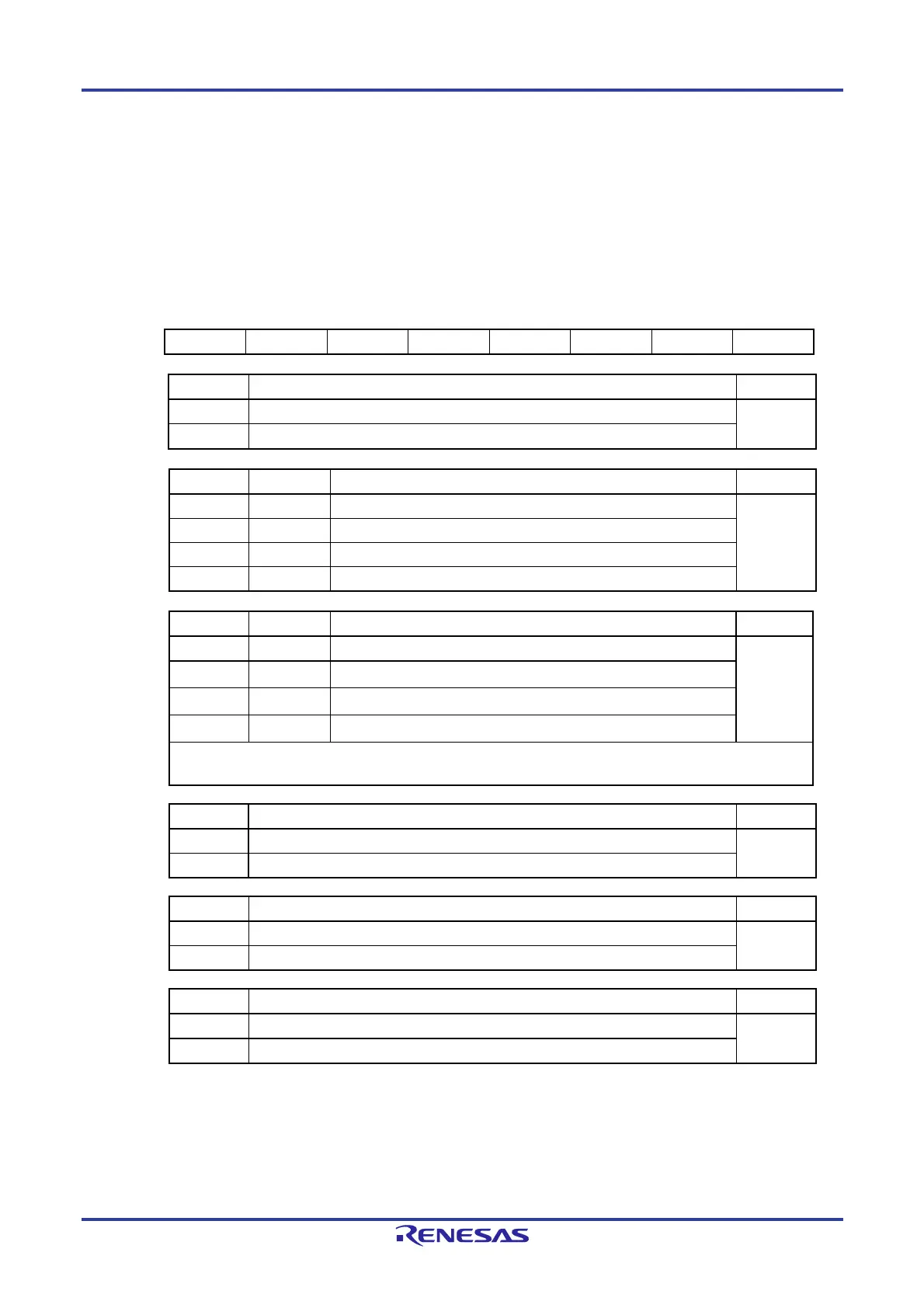
Figure 14-3. Format of Comparator Control Register (CMPCTL)
Address: F0341H After reset: 00H
Symbol <7> 6 5 4 3 2 <1> 0
CMPCTL HCMPON CDFS1 CDFS0 CEGN CEGP CSTEN COE CINV
HCMPON Comparator operation control
Note 1
R/W
0 Operation stopped (the comparator outputs a low-level signal) R/W
1 Operation enabled (input to the comparator pins is enabled)
CDFS1 CDFS0 Noise filter selection
Notes 2, 3, 4
R/W
0 0 Noise filter not used R/W
0 1 Noise filter sampling frequency is 2
3
/fCLK.
1 0 Noise filter sampling frequency is 2
4
fCLK.
1 1 Noise filter sampling frequency is 2
5
fCLK.
CEGN CEGP Selection of valid edge of INTCMP interrupt signal R/W
0 0 No edge selection R/W
0 1 Falling edge selection
1 0
Rising edge selection
1 1 Both-edge selection
The valid edge is set for the signal after the comparator polarity is selected by using the CINV bit and the filter is
selected by using CDFS1 and CDFS0 bits.
CSTEN STOP mode release enable
Notes 5, 6
R/W
0 Releasing STOP mode by comparator interrupt disabled R/W
1 Releasing STOP mode by comparator interrupt enabled
COE Comparator output enable R/W
0 Comparator output disabled (the output signal is low level) R/W
1 Comparator output enabled
CINV Comparator output polarity selection
Notes 2, 3, 6
R/W
0 Comparator output not inverted R/W
1 Comparator output inverted
Notes 1. Do not modify bits HCMPON and COE simultaneously. The operation stabilization wait time (1 µs
when 3.3 V ≤ VDD ≤ 5.5 V or 3 µs when 2.7 V ≤ VDD < 3.3 V) is required after enabling comparator
operation (HCMPON = 1).
2. Change bits CDFS1, CDFS0, CEGN, CEGP, CSTEN and CINV only after disabling the
comparator output (COE = 0).
3. Changes to the values of the CDFS1, CDFS0, CEGN, CEGP, CSTEN, and CINV bits may lead to
a comparator interrupt request, ELC event request, DTC transfer request, or setting of the
INTFLG06 bit in the interrupt source determination flag register 0. Change these bits only after
 Loading...


