RL78/F13, F14 CHAPTER 7 TIMER RJ
R01UH0368EJ0210 Rev.2.10 553
Dec 10, 2015
7.3.7 Timer RJ Mode Register 0 (TRJMR0)
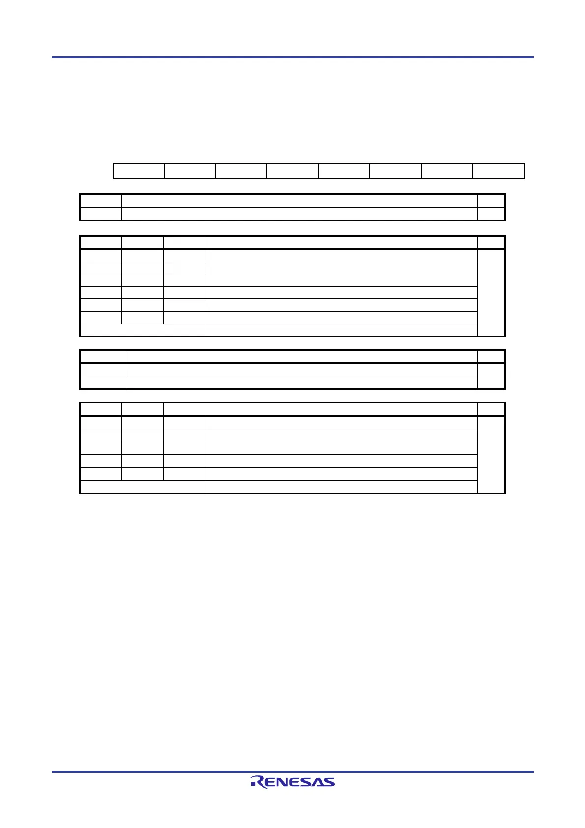
Figure 7-8. Format of Timer RJ Mode Register 0 (TRJMR0)
Address : F0242H After Reset: 00H
Symbol 7 6 5 4 3 2 1 0
TRJMR0 — TCK2 TCK1 TCK0 TEDGPL TMOD2 TMOD1 TMOD0
Bit 7 Nothing is assigned R/W
— The write value must be 0. The read value is 0. R
TCK2 TCK1 TCK0
Timer RJ count source select
Notes 1, 2
R/W
0 0 0 fCLK R/W
0 0 1 fCLK/8
0 1 1 fCLK/2
1 0 0
f
IL
Note 4
1 0 1
Event input from event link controller (ELC)
Note 5
1 1 0 fSL
Other than above Setting prohibited
TEDGPL
TRJIO0 edge polarity select
Note 6
R/W
0 One edge R/W
1 Both edges
TMOD2 TMOD1 TMOD0
Timer RJ operating mode select
Note 3
R/W
0 0 0 Timer mode R/W
0 0 1
Pulse output mode
Note 7
0 1 0
Event counter mode
Note 7
0 1 1
Pulse width measurement mode
Note 7
1 0 0
Pulse period measurement mode
Note 7
Other than above Setting prohibited
Notes 1. When event counter mode is selected, the external input (TRJIO0) is selected as the count source regardless
of the setting of bits TCK0 to TCK2.
2. Do not switch count sources during count operation. When switching count sources, set the TSTART and
TCSTF bits in the TRJCR0 register to 0 (count stops).
3. The operating mode can be changed only when the count is stopped while both the bits TSTART and TCSTF
in the TRJCR0 register are set to 0 (count stops). Do not change the operating mode during count operation.
4. When selecting f
IL as the count source, set the WUTMMCK0 bit in the operation speed mode register
(OSMC) to 1.
However, fSUB cannot be selected as the count source for timer RJ when the SELLOSC bit in the CKSEL
register is set to 1.
5. Only available in the RL78/F14. Do not make the setting in other products.
6. The TEDGPL bit is enabled only in event counter mode.
7. The 20-pin products do not have TRJIO0 and TRJO0 pins. Thus, the pulse output mode, event counter mode,
pulse width measurement mode, and pulse period measurement mode cannot be used.
Caution Write access to the TRJMR0 register initializes the output from pins TRJO0 and TRJIO0 of timer RJ.
For details on the output level at initialization, refer to the description shown below Figure 7-7 Format
of Timer RJ I/O Control Register 0 (TRJIOC0).
 Loading...


