RL78/F13, F14 CHAPTER 12 A/D CONVERTER
R01UH0368EJ0210 Rev.2.10 730
Dec 10, 2015
12.3.14 Port mode control registers 7, 9, and 12 (PMC7, PMC9, PMC12)
These registers are used to switch the ANI24 to ANI30 pins between the analog input of the A/D converter and the digital
I/O of the port.
The PMC7, PMC9, and PMC12 registers can be set by a 1-bit or 8-bit memory manipulation instruction.
Reset signal generation sets these registers to FFH.
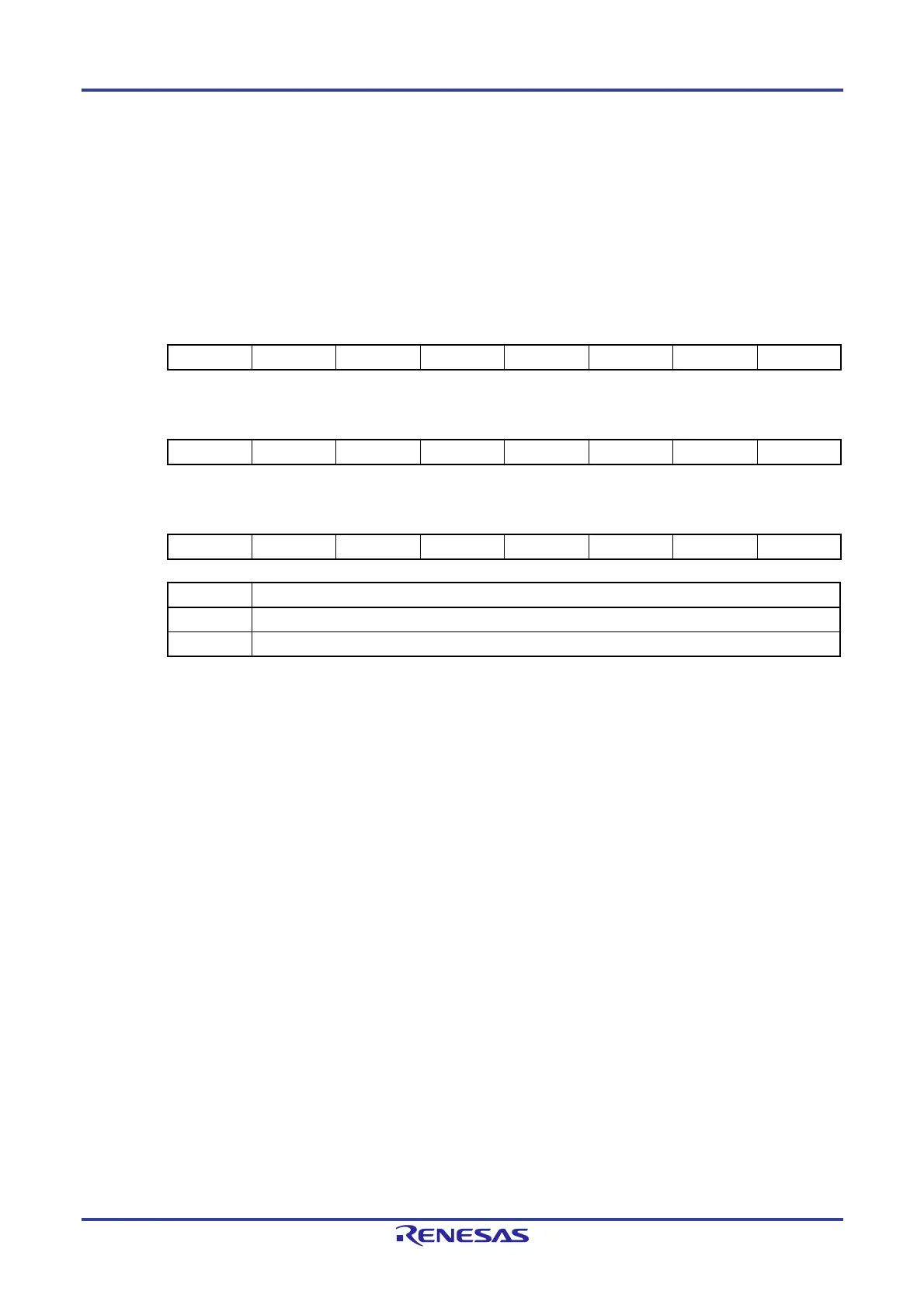
Figure 12-18. Formats of Port Mode Control Registers 7, 9, and 12 (PMC7, PMC9, PMC12)
Address: F0067H After reset: FFH R/W
Symbol 7 6 5 4 3 2 1 0
PMC7 1 1 1 PMC74
Note 1
PMC73
Note 1
PMC72
Note 1
PMC71
Note 1
PMC70
Address: F0069H After reset: FFH R/W
Symbol 7 6 5 4 3 2 1 0
PMC9 PMC97
Note 2
PMC96
Note 2
1 1 1 1 1 1
Address: F006CH After reset: FFH R/W
Symbol 7 6 5 4 3 2 1 0
PMC12 1 1 PMC125 1 1 1 1 PMC120
PMC Digital I/O/analog input selection
0 Digital I/O (dual-use function other than analog input)
1 Analog input
Notes 1. Be sure to clear the following bits to 0.
PMC71 to PMC74 bits in the RL78/F14 products with 64 pins and 128 Kbytes to 256 Kbytes of
code flash memory.
PMC73 bit in the RL78/F14 products with 48 pins and 128 Kbytes to 256 Kbytes of code flash
memory.
2. The ADPC and PMC9 registers are used to select the digital I/O or analog input functions for the
P96/ANI16 and P97/ANI17 pins and for the P96/ANI26 and P97/ANI27 pins, respectively. For details
on pin functions allocated to each product, see 1.5 Pin Configurations.
Cautions 1. Set port pins specified as analog input pins to input mode by using port mode register x
(PMx).
2. Be sure to set bits for pins that are not present to their initial values , and see Note 1 for
PMC71 to PMC74.
<R>
<R>
 Loading...


