RL78/F13, F14 CHAPTER 8 TIMER RD
R01UH0368EJ0210 Rev.2.10 590
Dec 10, 2015
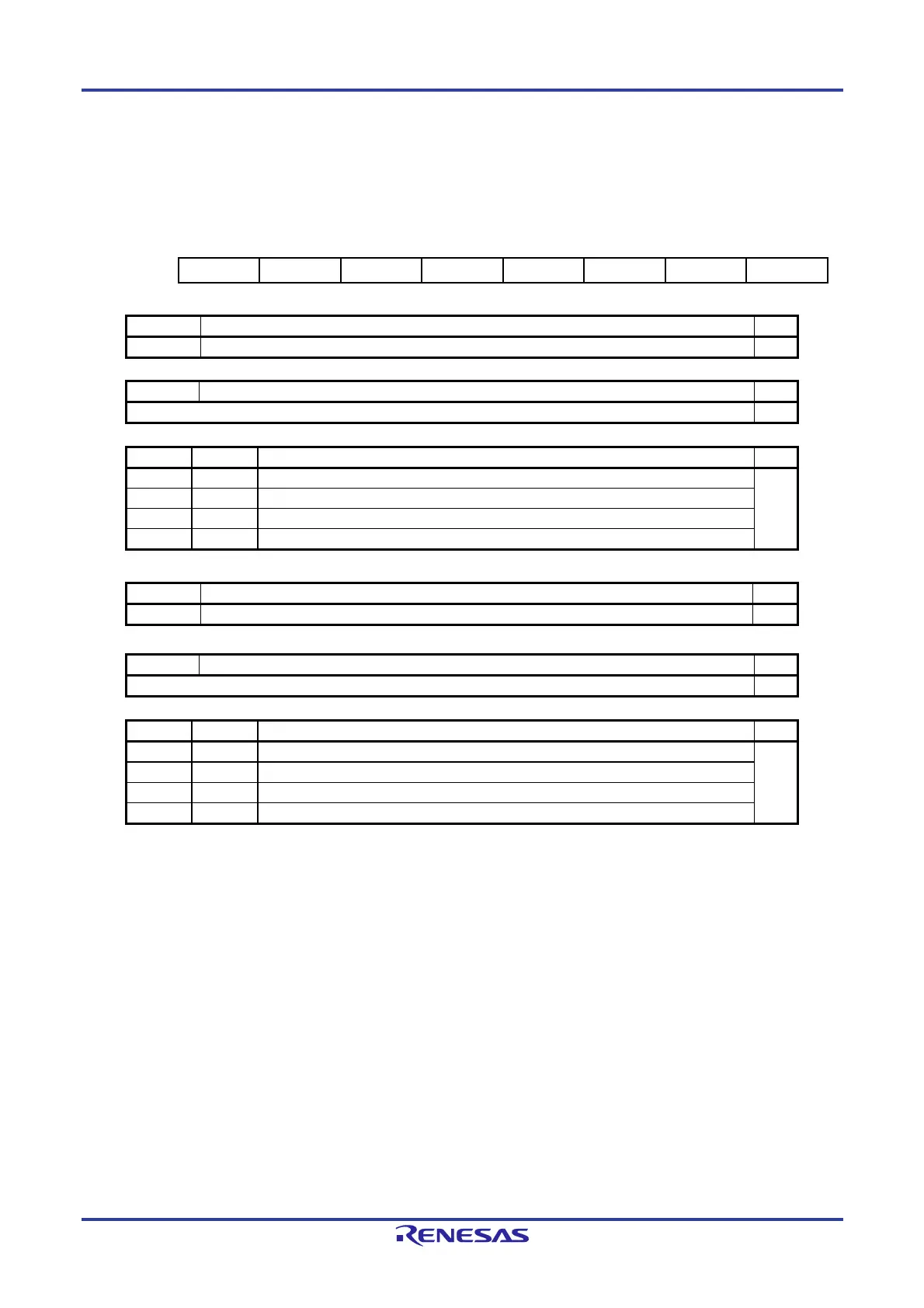
8.2.13 Timer RD I/O Control Register Ai (TRDIORAi) (i = 0 or 1)
Figure 8-21. Format of Timer RD I/O Control Register Ai (TRDIORAi) (i = 0 or 1) [Input Capture Function]
Address: F0271H (TRDIORA0), F0281H (TRDIORA1) After Reset: 00H
Note 1
Symbol 7 6 5 4 3 2 1 0
TRDIORAi — IOB2 IOB1 IOB0 0 IOA2 IOA1 IOA0
IOB2
TRDGRBi mode select
Note 2
R/W
Set to 1 (input capture) in the input capture function. R/W
IOB1 IOB0 TRDGRBi control R/W
0 0 Input capture to TRDGRBi at the rising edge R/W
0 1 Input capture to TRDGRBi at the falling edge
1 0 Input capture to TRDGRBi at both edges
1 1 Do not set.
IOA2
TRDGRAi mode select
Note 3
R/W
Set to 1 (input capture) in the input capture function. R/W
IOA1 IOA0 TRDGRAi control R/W
0 0 Input capture to TRDGRAi at the rising edge R/W
0 1 Input capture to TRDGRAi at the falling edge
1 0 Input capture to TRDGRAi at both edges
1 1 Do not set.
Notes 1. The value after reset is undefined when FRQSEL4 = 1 in the user option byte (000C2H/020C2H) and
TRD0EN = 0 in the PER1 register. If it is necessary to read the initial value, set f
CLK to fIH and TRD0EN =
1 before reading.
2. If 1 (buffer register for TRDGRBi register) is selected for the TRDBFDi bit in the TRDMR register, set the
same value to the IOB2 bit in the TRDIORAi register and the IOD2 bit in the TRDIORCi register.
3. If 1 (buffer register for TRDGRAi register) is selected for the TRDBFCi bit in the TRDMR register, set the
same value to the IOA2 bit in the TRDIORAi register and the IOC2 bit in the TRDIORCi register.
Bit 7 Nothing is assigned R/W
— The write value must be 0. The read value is 0. R
Bit 3 Reserved R/W
0 Set to 0. R/W
 Loading...


