RL78/F13, F14 CHAPTER 12 A/D CONVERTER
R01UH0368EJ0210 Rev.2.10 742
Dec 10, 2015
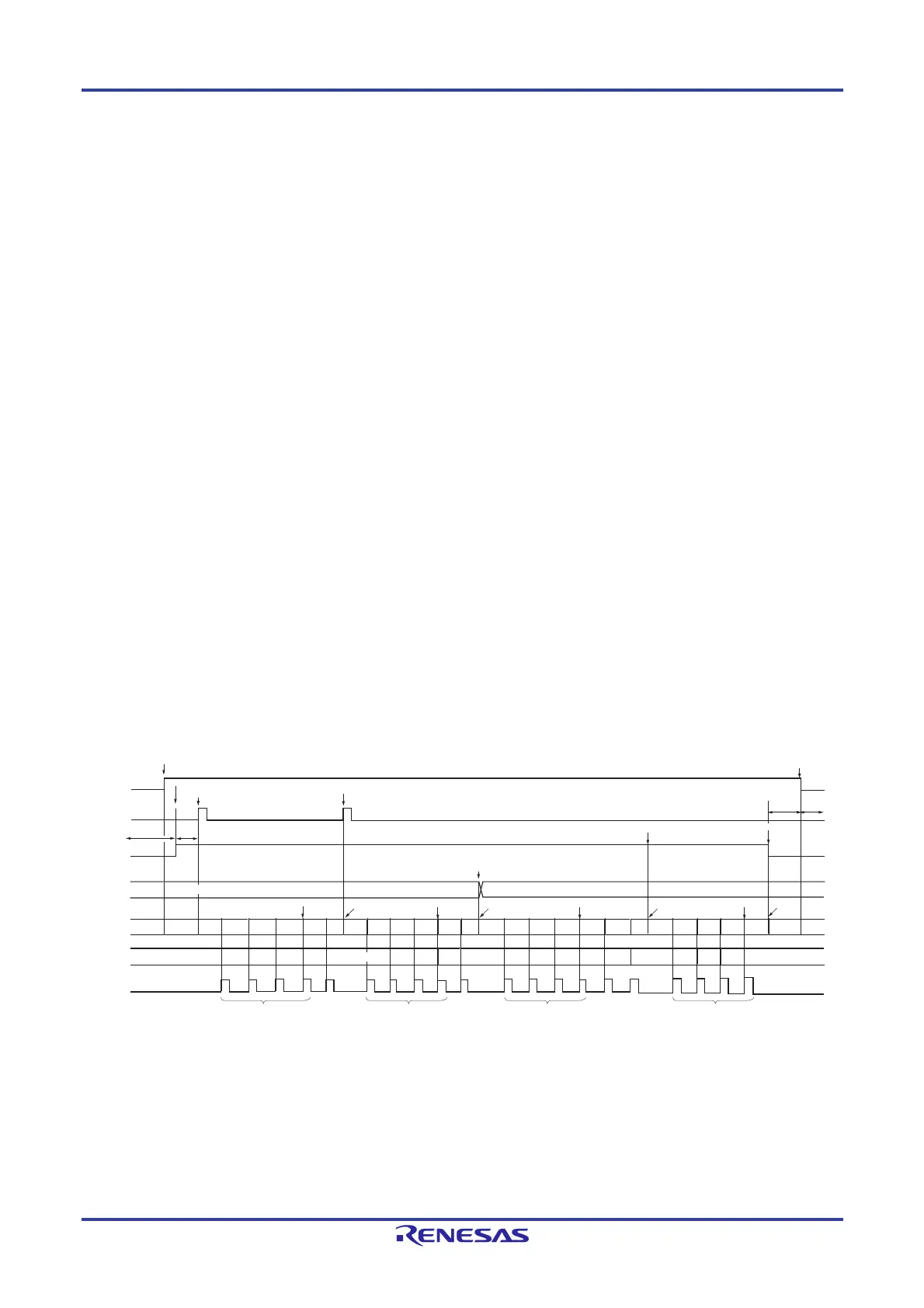
12.6.7 Hardware trigger no-wait mode (scan mode, sequential conversion mode)
<1> In the stop status, the ADCE bit of A/D converter mode register 0 (ADM0) is set to 1, and the system enters the
A/D conversion standby status.
<2> After the software counts up to the stabilization wait time (1 s), the ADCS bit of the ADM0 register is set to 1 to
place the system in the hardware trigger standby status (and conversion does not start at this stage). Note that,
while in this status, A/D conversion does not start even if ADCS is set to 1.
<3> If a hardware trigger is input while ADCS = 1, A/D conversion is performed on the four analog input channels
specified by scan 0 to scan 3, which are specified by the analog input channel specification register (ADS). A/D
conversion is performed on the analog input channels in order, starting with that specified by scan 0.
<4> A/D conversion is sequentially performed on the four analog input channels, the conversion results are stored in
the A/D conversion result register (ADCR, ADCRH) each time conversion ends, and the A/D conversion end
interrupt request signal (INTAD) is generated. After A/D conversion of the four channels ends, the A/D conversion
of the channel following the specified channel automatically starts.
<5> If a hardware trigger is input during conversion operation, the current A/D conversion is interrupted, and conversion
restarts at the first channel. The partially converted data is discarded.
<6> When the value of the ADS register is rewritten or overwritten during conversion operation, the current A/D
conversion is interrupted, and A/D conversion is performed on the first channel respecified by the ADS register.
The partially converted data is discarded.
<7> When ADCS is overwritten with 1 during conversion operation, the current A/D conversion is interrupted, and
conversion restarts. The partially converted data is discarded.
<8> When ADCS is cleared to 0 during conversion operation, the current A/D conversion is interrupted, and the system
enters the A/D conversion standby status. However, the A/D converter does not stop in this status.
<9> When ADCE is cleared to 0 while in the A/D conversion standby status, the A/D converter enters the stop status.
When ADCE = 0, specifying 1 for ADCS is ignored and A/D conversion does not start.
Figure 12-28. Example of Hardware Trigger No-Wait Mode (Scan Mode, Sequential Conversion Mode) Operation
Timing
ADCE
ADCS
ADS
INTAD
ADCR,
ADCRH
A/D
conversion
status
ADCE is set to 1.
<1>
ADCE is cleared to 0.
<9>
The trigger is not
acknowledged.
Conversion
standby
Stop
status
Conversion
standby
Stop
status
Data 1
(ANI0)
Data 1
(ANI0)
Data 2
(ANI1)
Data 2
(ANI1)
Data 3
(ANI2)
Data 3
(ANI2)
Data 4
(ANI3)
Data 1
(ANI0)
Data 2
(ANI1)
Data 6
(ANI5)
Data 6
(ANI5)
Data 6
(ANI5)
Data 6
(ANI5)
Data 5
(ANI4)
Data 5
(ANI4)
Data 5
(ANI4)
Data 5
(ANI4)
Data 5
(ANI4)
Data 5
(ANI4)
Data 5
(ANI4)
Data 6
(ANI5)
Data 6
(ANI5)
Data 2
(ANI1)
Data 3
(ANI2)
Data 3
(ANI2)
Data 4
(ANI3)
Data 1
(ANI0)
Data 4
(ANI3)
Data 8
(ANI7)
Data 8
(ANI7)
Data 8
(ANI7)
Data 8
(ANI7)
Data 7
(ANI6)
Data 7
(ANI6)
Data 7
(ANI6)
Data 7
(ANI6)
Data 4
(ANI3)
Data 1
(ANI0)
Data 1
(ANI0)
Data 2
(ANI1)
Data 2
(ANI1)
Data 7
(ANI6)
Conversion is
interrupted
and restarts.
Conversion is
interrupted
and restarts.
Conversion is
interrupted.
Conversion is
interrupted
and restarts.
A/D conversion
ends and the next
conversion starts.
<4>
<4> <4><4>
ADS is rewritten during
A/D conversion operation.
<6>
The interrupt is generated four times. The interrupt is generated four times. The interrupt is generated four times. The interrupt is generated four times.
Trigger
standby
status
Hardware
trigger
ADCS is set to 1.
<2>
A hardware trigger
is generated.
<3>
A hardware trigger is
generated during A/D
conversion operation.
<5>
ADCS is overwritten
with 1 during A/D
conversion operation.
<7>
ADCS is cleared to 0
during A/D conversion
operation.
Trigger
standby
status
<8>
The trigger
is not
acknowledged.
Data 1 (ANI0)
ANI0 to ANI3
ANI4 to ANI7
 Loading...


