RL78/F13, F14 CHAPTER 8 TIMER RD
R01UH0368EJ0210 Rev.2.10 612
Dec 10, 2015
8.2.21 Port mode registers (PM1, PM3, PM12)
These registers set input/output of port in 1-bit units. PM1, PM3, and PM12 are used in timer RD.
When using the ports (P13/TRDIOA0, P16/TRDIOC1, etc.) to be shared with the timer output pin for timer output, set the
bit in the port mode register (PMxx) and the bit in the port register (Pxx) corresponding to each port to 0.
Example: When using P13/TRDIOA0 for timer output
Set the PM13 bit of port mode register 1 to 0.
Set the P13 bit of port register 1 to 0.
When using the ports (P13/TRDIOA0, P16/TRDIOC1, etc.) to be shared with the timer input pin for timer input, set the
bit in the port mode register (PMxx) corresponding to each port to 1. At this time, the bit in the port register (Pxx) may be 0
or 1.
Example: When using P13/TRDIOA0 for timer input
Set the PM13 bit of port mode register 1 to 1.
Set the P13 bit of port register 1 to 0 or 1.
The PM1, PM3, and PM12 registers can be set by a 1-bit or 8-bit memory manipulation instruction.
Reset signal generation sets this register to FFH.
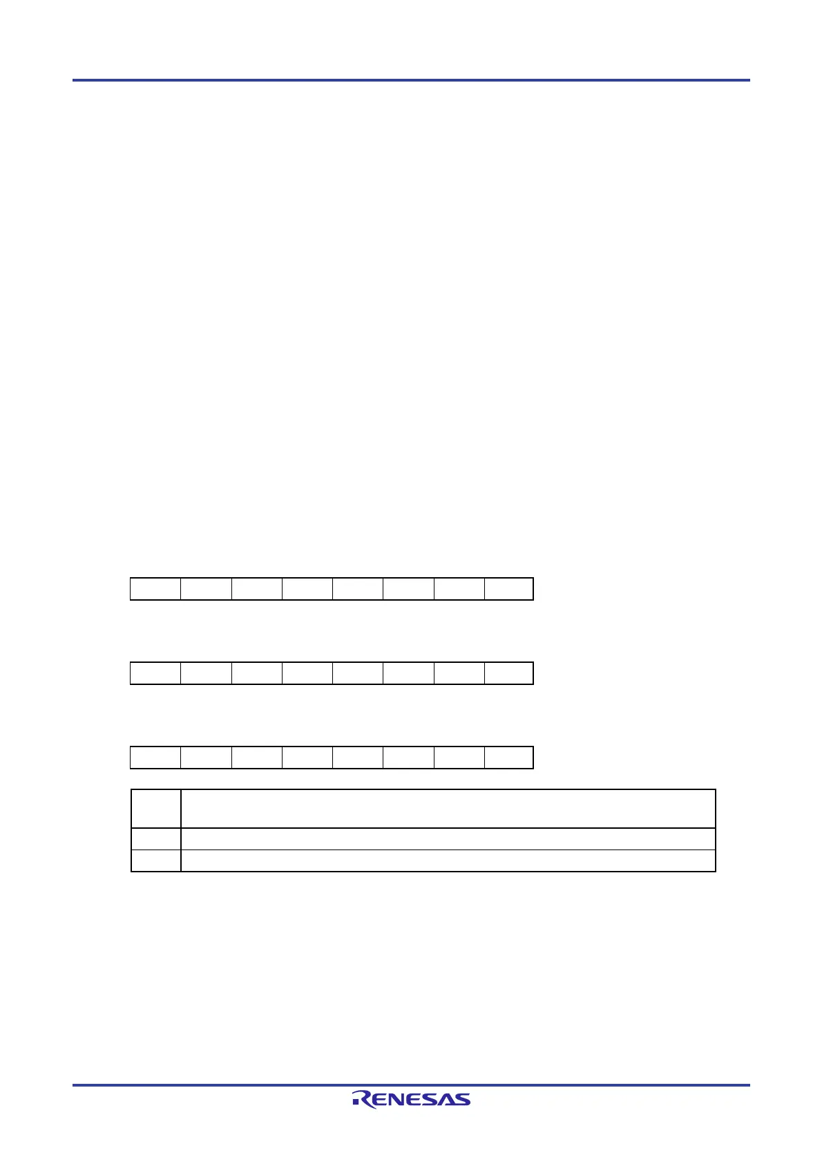
Figure 8-39. Format of Port Mode Registers (PM1, PM3, PM12) (100-pin products)
Address: FFF21H After reset: FFH R/W
Symbol 7 6 5 4 3 2 1 0
PM1 PM17 PM16 PM15 PM14 PM13 PM12 PM11 PM10
Address: FFF23H After reset: FFH R/W
Symbol 7 6 5 4 3 2 1 0
PM3 1 1 1 PM34 PM33 PM32 PM31 PM30
Address: FFF2CH After reset: FFH R/W
Symbol 7 6 5 4 3 2 1 0
PM12 PM127 PM126 PM125 1 1 1 1 PM120
PMmn
Pmn pin I/O mode selection
(m = 1, 3, 12; n = 0 to 7)
0 Output mode (output buffer on)
1 Input mode (output buffer off)
Remark The figure shown above presents the format of port mode registers of the 100-pin products.
 Loading...


