RL78/F13, F14 CHAPTER 8 TIMER RD
R01UH0368EJ0210 Rev.2.10 579
Dec 10, 2015
8.2.9 Timer RD Output Master Enable Register 2 (TRDOER2)
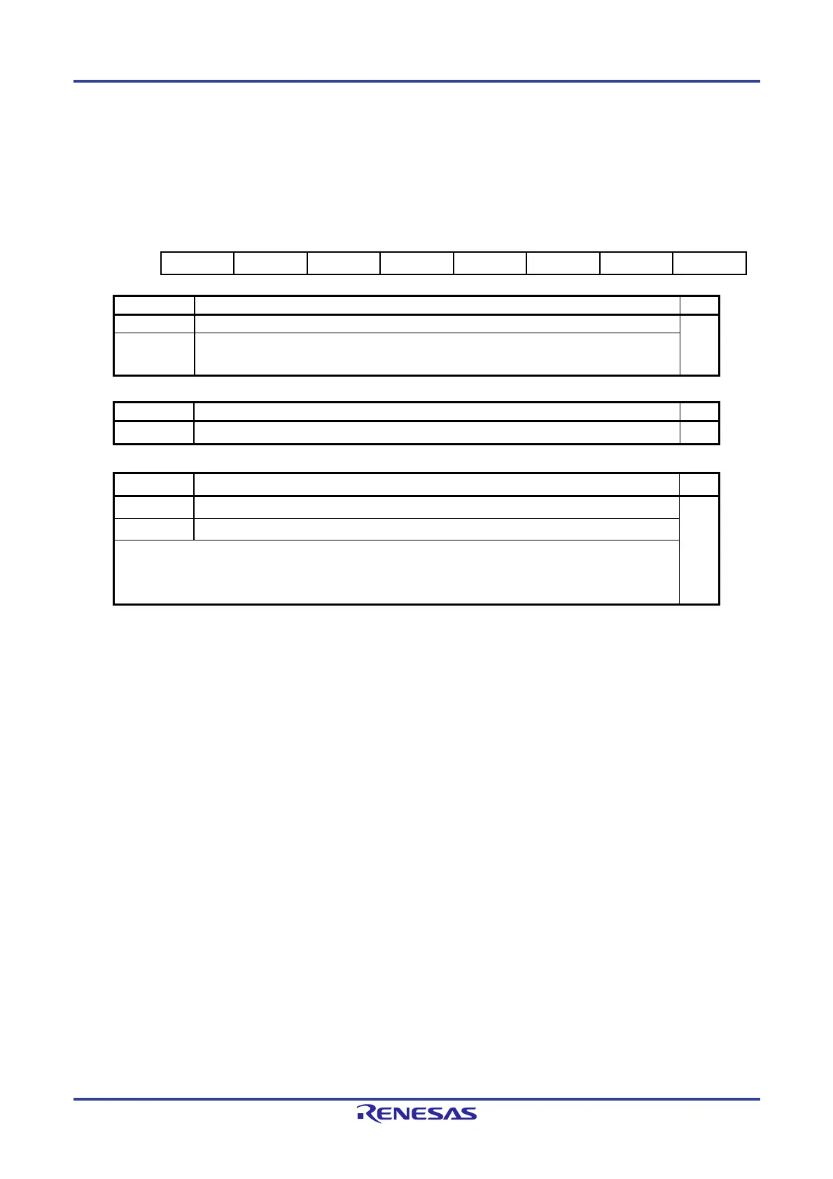
Figure 8-10. Format of Timer RD Output Master Enable Register 2 (TRDOER2)
[PWM Function, Reset Synchronous PWM Mode, Complementary PWM Mode, and PWM3 Mode]
Address: F0268H After Reset: 00H
Note 1
Symbol <7> 6 5 4 3 2 1 <0>
TRDOER2 TRDPTO 0 0 0 0 0 0 TRDSHUTS
TRDPTO
INTP0 of pulse output forced cutoff signal input enabled
Note 2
R/W
0 Pulse output forced cutoff input disabled R/W
1
Pulse output forced cutoff input enabled
(The TRDSHUTS bit is set to 1 when a low level is applied to the INTP0 pin.)
TRDSHUTS Forced cutoff flag R/W
0 Not forcibly cut off R/W
1 Forcibly cut off
This bit is set to 1 when the pulse is forcibly cut off by an INTP0 or ELC
Note 3
input event. This bit is not
automatically cleared. To stop the forced cutoff of the pulse, write 0 to this bit while the count is stopped
(TSTARTi = 0). The pulse is also forcibly cut off when 1 is written to the TRDSHUTS bit in an enabled mode.
Notes 1. The value after reset is undefined when FRQSEL4 = 1 in the user option byte (000C2H/020C2H) and
TRD0EN = 0 in the PER1 register. If it is necessary to read the initial value, set f
CLK to fIH and TRD0EN
= 1 before reading.
2. See 8.3.1 (4) Pulse Output Forced Cutoff.
3. The ELC is only available in the RL78/F14.
Bits 6 to 1 Nothing is assigned R/W
—
The write value must be 0. The read value is 0.
R
 Loading...


