RL78/F13, F14 CHAPTER 21 INTERRUPT FUNCTIONS
R01UH0368EJ0210 Rev.2.10 1503
Dec 10, 2015
21.3.7 Input switch control register (ISC)
The ISC0 bit of the ISC register is used for the LIN-bus communication with UART0. The ISC2 and ISC3 bits are used
for the LIN/UART module (RLIN3). When the ISC0 bit is set to 1, set the TIS17 and TIS16 bits in the TIS1 register (timer
input select register 1) at the same time.
Setting bit 0 to 1 selects the input signal of the serial data input pin (RxD0) as the external interrupt input (INTP0), which
allows detection of the wakeup signal by the INTP0 interrupt.
Setting bits 2 and 3 to 1 select the input signal of the serial data input pin (RxD0) for the LIN/UART module as the external
interrupt input.
This register can be set by an 8-bit memory manipulation instruction.
Reset signal generation sets this register to 00H.
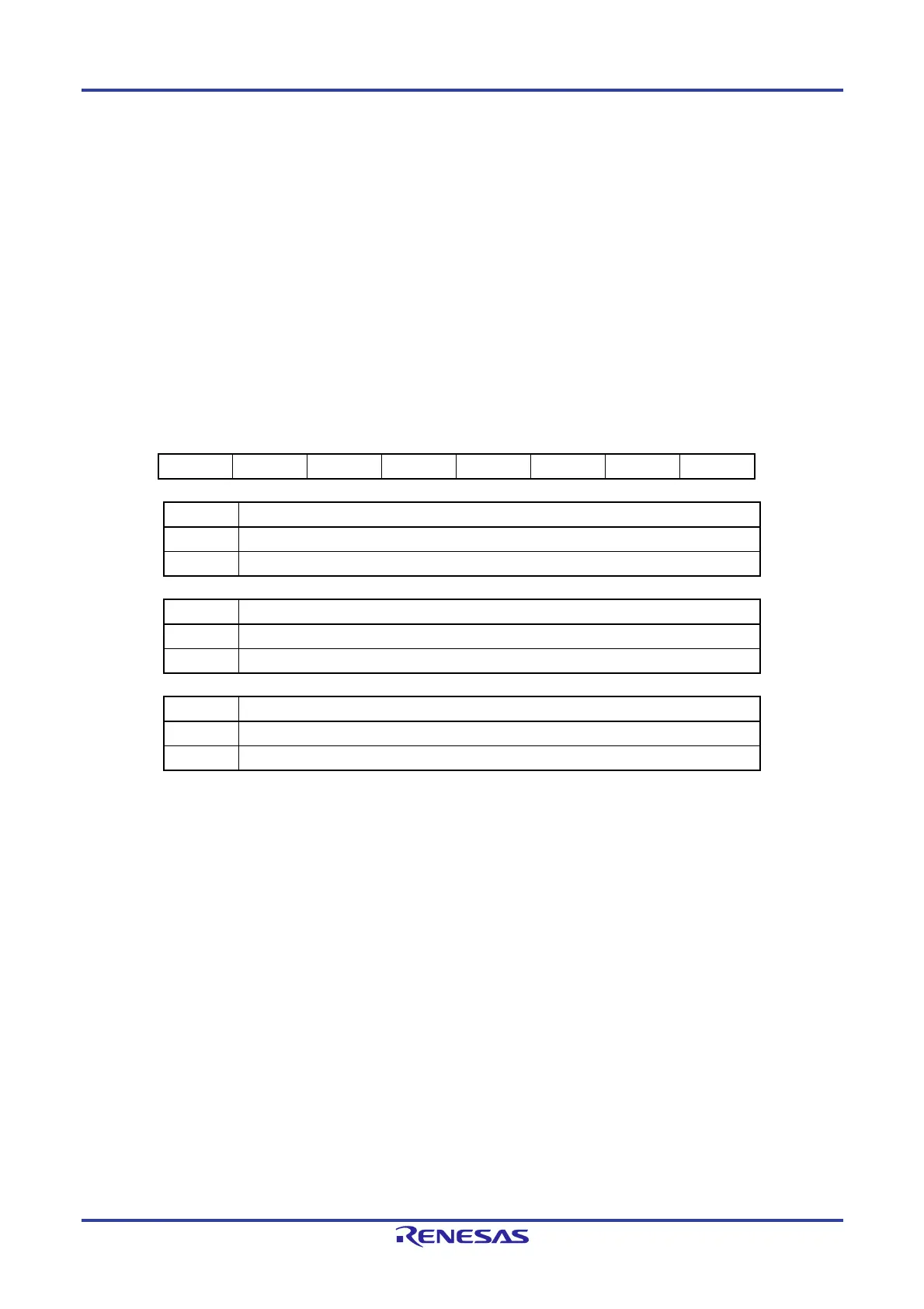
Figure 21-9. Format of Input Switch Control Register (ISC)
ddress: F0073H After reset: 00H R/W
Symbol 7 6 5 4 <3> <2> 1 <0>
ISC 0 0 0 0 ISC3 ISC2 0 ISC0
ISC3 Input selection for external interrupt INTP12
0 INTP12 pin input signal is selected as external interrupt input.
1 LRxD1 pin input signal is selected as external interrupt input.
ISC2 Input selection for external interrupt INTP11
0 INTP11 pin input signal is selected as external interrupt input.
1 LRxD0 pin input signal is selected as external interrupt input.
ISC0 Input selection for external interrupt INTP0
0 INTP0 pin input signal is selected as external interrupt input. (normal operation)
1 RxD0 pin input signal is selected as external interrupt input. (wake-up signal detection)
Caution Bits 7 to 4 and 1 should always be set to 0.
 Loading...


