RL78/F13, F14 CHAPTER 8 TIMER RD
R01UH0368EJ0210 Rev.2.10 598
Dec 10, 2015
8.2.16 Timer RD Interrupt Enable Register i (TRDIERi) (i = 0 or 1)
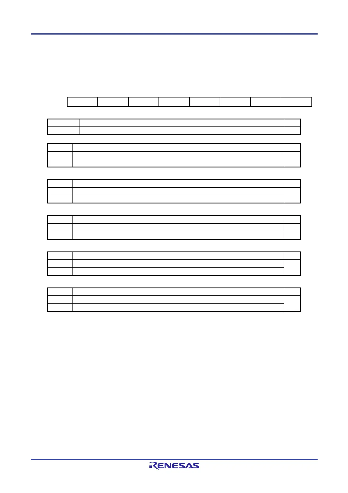
Figure 8-27. Format of Timer RD Interrupt Enable Register i (TRDIERi) (i = 0 or 1)
Address: F0274H (TRDIER0), F0284H (TRDIER1) After Reset: 00H
Note
Symbol 7 6 5 4 3 2 1 0
TRDIERi — — — OVIE IMIED IMIEC IMIEB IMIEA
OVIE Overflow/underflow interrupt enable R/W
0 Interrupt (OVI) by bits OVF and UDF disabled R/W
1 Interrupt (OVI) by bits OVF and UDF enabled
IMIED Input capture/compare match interrupt enable D R/W
0 Interrupt (IMID) by the IMFD bit is disabled R/W
1 Interrupt (IMID) by the IMFD bit is enabled
IMIEC Input capture/compare match interrupt enable C R/W
0 Interrupt (IMIC) by the IMFC bit is disabled R/W
1 Interrupt (IMIC) by the IMFC bit is enabled
IMIEB Input capture/compare match interrupt enable B R/W
0 Interrupt (IMIB) by the IMFB bit is disabled R/W
1 Interrupt (IMIB) by the IMFB bit is enabled
IMIEA Input capture/compare match interrupt enable A R/W
0 Interrupt (IMIA) by the IMFA bit is disabled R/W
1 Interrupt (IMIA) by the IMFA bit is enabled
Note The value after reset is undefined when FRQSEL4 = 1 in the user option byte (000C2H/020C2H) and TRD0EN
= 0 in the PER1 register. If it is necessary to read the initial value, set f
CLK to fIH and TRD0EN = 1 before reading.
Bits 7 to 5 Nothing is assigned R/W
— The write value must be 0. The read value is 0. R
 Loading...


