RL78/F13, F14 CHAPTER 12 A/D CONVERTER
R01UH0368EJ0210 Rev.2.10 717
Dec 10, 2015
12.3.4 A/D converter mode register 2 (ADM2)
This register is used to select the A/D converter reference voltage, check the upper limit and lower limit A/D conversion
result values, select the resolution, and specify whether to use the SNOOZE mode.
The ADM2 register can be set by a 1-bit or 8-bit memory manipulation instruction.
Reset signal generation clears this register to 00H.
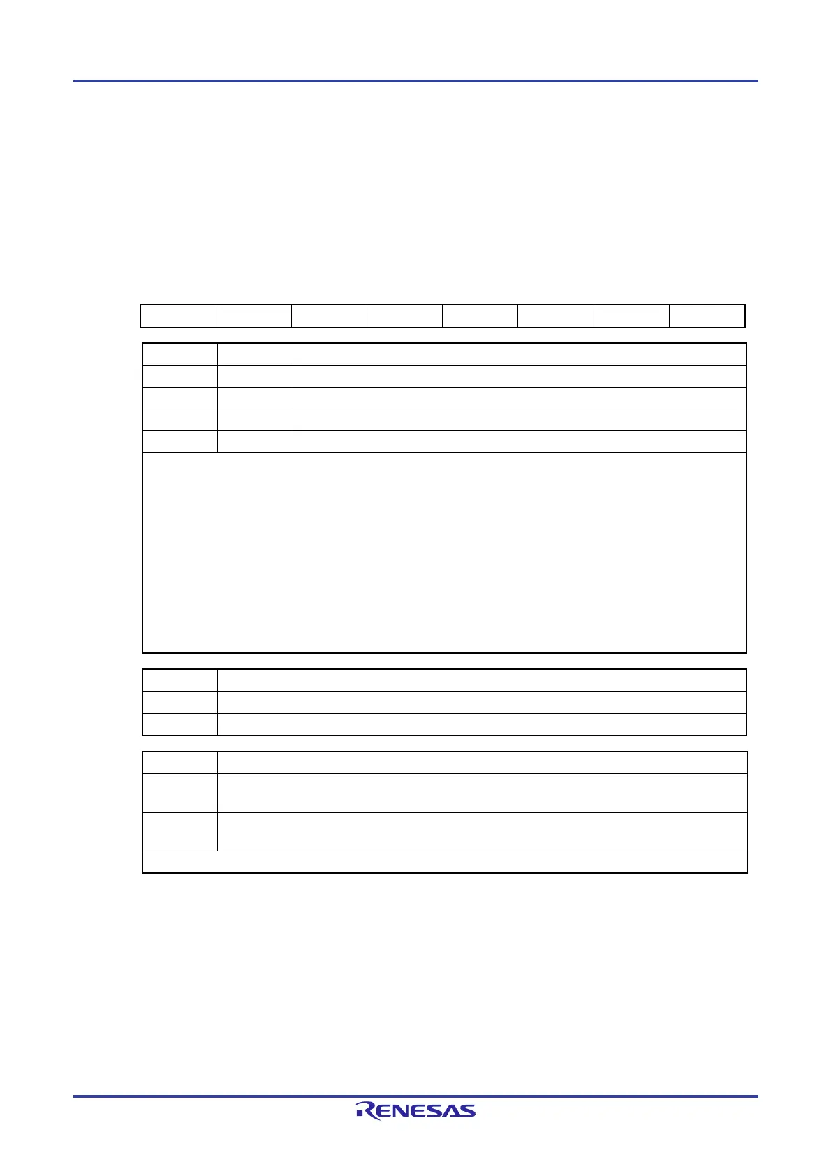
Figure 12-7. Format of A/D Converter Mode Register 2 (ADM2) (1/2)
Address: F0010H After reset: 00H R/W
Symbol 7 6 5 4 <3> <2> 1 <0>
ADM2 ADREFP1 ADREFP0 ADREFM 0 ADRCK AWC 0 ADTYP
ADREFP1 ADREFP0 Selection of the + side reference voltage source of the A/D converter
0 0 Supplied from VDD
0 1 Supplied from P33/AVREFP/ANI0
1 0 Supplied from the internal reference voltage (1.45 V)
1 1 Setting prohibited
When ADREFP1 or ADREFP0 bit is rewritten, this must be configured in accordance with the following procedures.
(1) Set ADCE = 0
(2) Change the values of ADREFP1 and ADREFP0
(3) Stabilization wait time (A)
(4) Set ADCE = 1
(5) Stabilization wait time (B)
When ADREFP1 and ADREFP0 are set to 1 and 0, the setting is changed to A = 5 s, B = 1 s.
When ADREFP1 and ADREFP0 are set to 0 and 0 or 0 and 1, A needs no wait and B = 1 s.
Start A/D conversion after the wait time (5) specified above).
When ADREFP1 and ADREFP0 are set to 1 and 0, respectively, A/D conversion cannot be performed on the
temperature sensor output and internal reference voltage output.
Be sure to perform A/D conversion while ADISS = 0.
ADREFM Selection of the side reference voltage source of the A/D converter
0 Supplied from VSS
1 Supplied from P34/AVREFM/ANI1
ADRCK Checking the upper limit and lower limit conversion result values
0
The interrupt signal (INTAD) is output when the ADLL register the ADCR register the ADUL register
(<1>).
1
The interrupt signal (INTAD) is output when the ADCR register < the ADLL register (<2>) or the ADUL
register < the ADCR register (<3>).
Figure 12-8 shows the generation range of the interrupt signal (INTAD) for <1> to <3>.
Cautions 1. Only rewrite the value of the ADM2 register while conversion operation is stopped (which is
indicated by the ADCS bit of A/D converter mode register 0 (ADM0) being 0).
2. When entering STOP mode or HALT mode while the CPU is operating on the subsystem/low-
speed on-chip oscillator select clock, do not set ADREFP1 to 1. When the internal reference
voltage is selected (ADREFP1, ADREFP0 = 1, 0), the current value defined in the supply
current characteristics in CHAPTER 34 to CHAPTER 36 ELECTRICAL SPECIFICATIONS must
be added.
3. When using AV
REFP and AVREFM, specify ANI0 and ANI1 as the analog input channels and
specify input mode by using the port mode register.
 Loading...


