RL78/F13, F14 CHAPTER 8 TIMER RD
R01UH0368EJ0210 Rev.2.10 594
Dec 10, 2015
8.2.15 Timer RD Status Register i (TRDSRi) (i = 0 or 1)
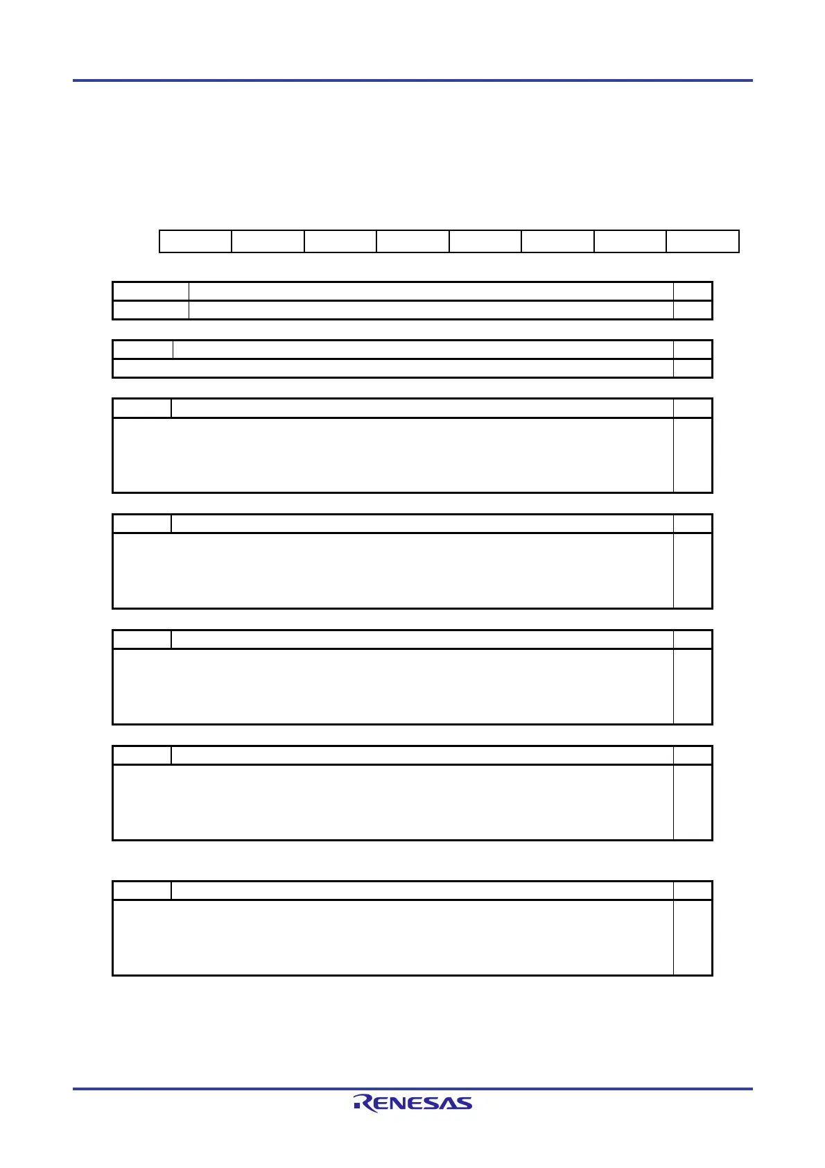
Figure 8-25. Format of Timer RD Status Register i (TRDSRi) (i = 0 or 1) [Input Capture Function]
Address: F0273H (TRDSR0), F0283H (TRDSR1) After Reset: 00H
Note 1
Symbol 7 6 5 4 3 2 1 0
TRDSRi — — UDF OVF IMFD IMFC IMFB IMFA
UDF
Underflow flag
Note 2
R/W
Disabled in the input capture function. R/W
OVF
Overflow flag
Note 3
R/W
[Source for setting to 0]
Write 0 after reading.
Note 4
[Source for setting to 1]
When the TRDi register overflows
R/W
IMFD
Input capture/compare match flag D
Note 7
R/W
[Source for setting to 0]
Write 0 after reading.
Note 4
[Source for setting to 1]
Input edge of TRDIODi pin
Note 5
R/W
IMFC
Input capture/compare match flag C
Note 7
R/W
[Source for setting to 0]
Write 0 after reading.
Note 4
[Source for setting to 1]
Input edge of TRDIOCi pin
Note 5
R/W
IMFB
Input capture/compare match flag B
Note 7
R/W
[Source for setting to 0]
Write 0 after reading.
Note 4
[Source for setting to 1]
Input edge of TRDIOBi pin
Note 6
R/W
IMFA
Input capture/compare match flag A
Note 7
R/W
[Source for setting to 0]
Write 0 after reading.
Note 4
[Source for setting to 1]
Input edge of TRDIOAi pin
Note 6
R/W
(Notes are listed on the next page.)
Bits 7 to 6 Nothing is assigned R/W
— The write value must be 0. The read value is 0. R
 Loading...


