RL78/F13, F14 CHAPTER 8 TIMER RD
R01UH0368EJ0210 Rev.2.10 593
Dec 10, 2015
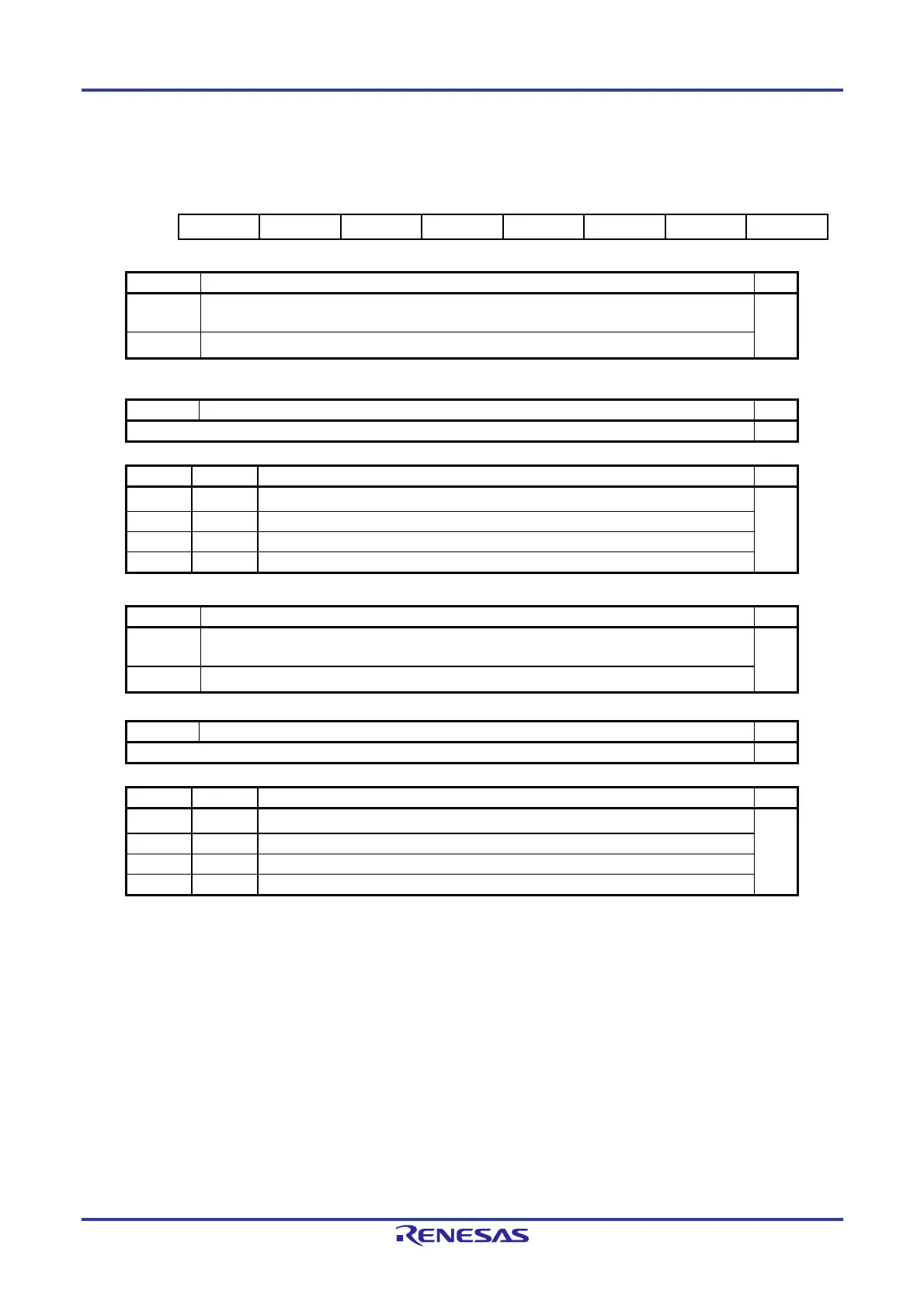
Figure 8-24. Format of Timer RD I/O Control Register Ci (TRDIORCi) (i = 0 or 1) [Output Compare Function]
Address: F0272H (TRDIORC0), F0282H (TRDIORC1) After Reset: 88H
Note 1
Symbol 7 6 5 4 3 2 1 0
TRDIORCi IOD3 IOD2 IOD1 IOD0 IOC3 IOC2 IOC1 IOC0
IOD2
TRDGRDi mode select
Note 2
R/W
Set to 0 (output compare) in the output compare function. R/W
IOD1 IOD0 TRDGRDi control R/W
0 0
Pin output by compare match is disabled
R/W
0 1 Low output by compare match with TRDGRDi
1 0 High output by compare match with TRDGRDi
1 1 Toggle output by compare match with TRDGRDi
IOC2
TRDGRCi mode select
Note 3
R/W
Set to 0 (output compare) in the output compare function. R/W
IOC1 IOC0 TRDGRCi control R/W
0 0
Pin output by compare match is disabled
R/W
0 1 Low output by compare match with TRDGRCi
1 0 High output by compare match with TRDGRCi
1 1 Toggle output by compare match with TRDGRCi
Notes 1. The value after reset is undefined when FRQSEL4 = 1 in the user option byte (000C2H/020C2H) and
TRD0EN = 0 in the PER1 register. If it is necessary to read the initial value, set f
CLK to fIH and TRD0EN =
1 before reading.
2. If 1 (buffer register for TRDGRBi register) is selected for the TRDBFDi bit in the TRDMR register, set the
same value to the IOB2 bit in the TRDIORAi register and the IOD2 bit in the TRDIORCi register.
3. If 1 (buffer register for TRDGRAi register) is selected for the TRDBFCi bit in the TRDMR register, set the
same value to the IOA2 bit in the TRDIORAi register and the IOC2 bit in the TRDIORCi register.
IOD3 TRDGRDi register function select R/W
0
TRDIOBi output register
(see 8.3.3 (2) Changing Output Pins in Registers TRDGRCi (i = 0 or 1) and TRDGRDi)
R/W
1
General register or buffer register
IOC3 TRDGRCi register function select R/W
0
TRDIOAi output register
(see 8.3.3 (2) Changing Output Pins in Registers TRDGRCi (i = 0 or 1) and TRDGRDi)
R/W
1
General register or buffer register
 Loading...


