RL78/F13, F14 CHAPTER 31 ON-CHIP DEBUG FUNCTION
R01UH0368EJ0210 Rev.2.10 1650
Dec 10, 2015
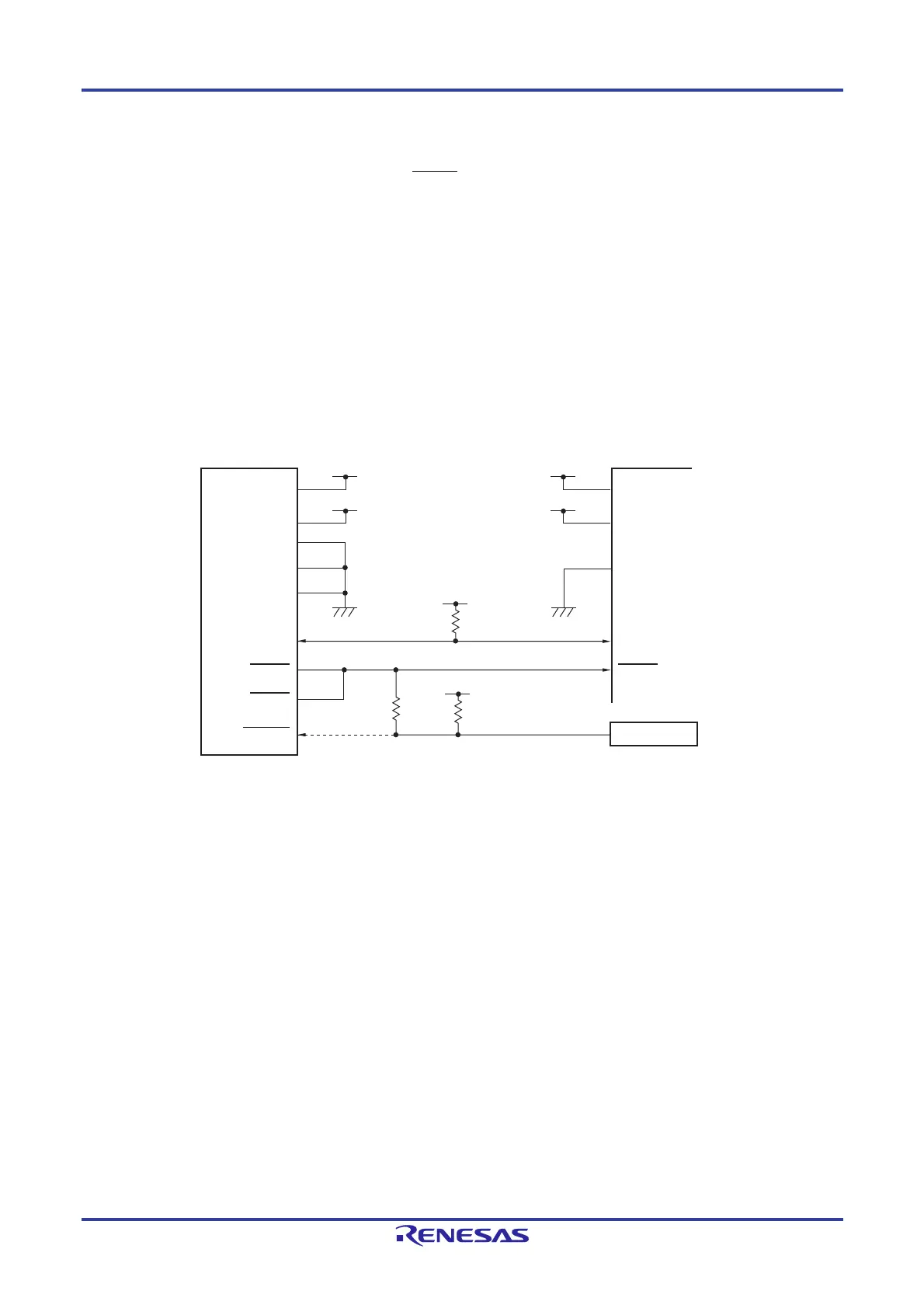
31.2 Connecting E1 On-chip Debugging Emulator to RL78/F13 or RL78/F14
The RL78/F13 and RL78/F14 use the V
DD, EVDD0, RESET, TOOL0, and VSS pins to communicate with the host machine
via an E1 on-chip debugging emulator. Serial communication is performed by using a single-line UART that uses the TOOL0
pin.
The RL78/F13 and RL78/F14 are provided with the hot plug-in detection function.
Caution The RL78/F13 and RL78/F14 have an on-chip debug function, which is provided for development and
evaluation. Do not use the on-chip debug function in products designated for mass production,
because the guaranteed number of rewritable times of the flash memory may be exceeded when this
function is used, and product reliability therefore cannot be guaranteed. Renesas Electronics is not
liable for problems occurring when the on-chip debug function is used.
Figure 31-2. Connection Example of E1 On-chip Debugging Emulator and RL78/F13 or RL78/F14
Notes 1. Connecting the dotted line is not necessary during flash programming.
2. If the reset circuit on the target system does not have a buffer and generates a reset signal only with resistors
and capacitors, this pull-up resistor is not necessary.
Caution This circuit diagram is assumed that the reset signal outputs from an N-ch O.D. buffer (output resistor:
100 or less)
E1 target connector
Note 2
Note 1
V
DD
TOOL0
V
DD
Reset circuit
Reset signal
GND
GND
GND
TOOL0
RESET
RESET
RESET
TRESET
V
DD
V
DD
V
DD
/EV
DD0
V
DD
/EV
DD0
10 kΩ
1 kΩ
1 kΩ
RL78/F13, RL78/F14
V
DD
EV
DD0
EV
DD0
EMVDD
V
SS
/EV
SS0
 Loading...


