RL78/F13, F14 CHAPTER 8 TIMER RD
R01UH0368EJ0210 Rev.2.10 644
Dec 10, 2015
(2) Transfer Timing from Buffer Register
Transfer from the TRDGRD0, TRDGRC1, or TRDGRD1 register to the TRDGRB0, TRDGRA1, or TRDGRB1
register.
When bits CMD1 and CMD0 in the TRDFCR register are set to 10B, the content is transferred when the TRD1
register underflows.
When bits CMD1 and CMD0 are set to 11B, the content is transferred at compare match between registers TRD0
and TRDGRA0.
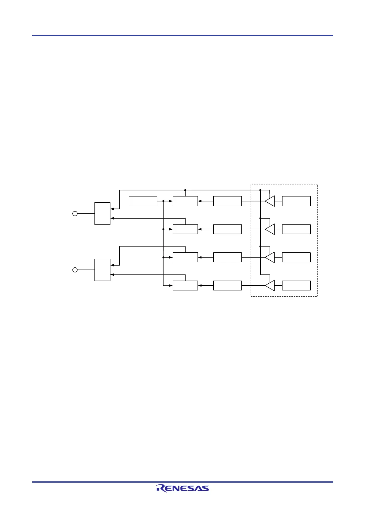
8.3.7 PWM3 Mode
In this mode, two PWM waveforms are output with the same period.
Figure 8-60 shows the Block Diagram of PWM3 Mode, Table 8-19 lists the PWM3 Mode Specifications, and Figure 8-61
shows an Operation Example in PWM3 Mode.
Figure 8-60. Block Diagram of PWM3 Mode
TRDIOA0
TRDGRC0
TRDIOB0
TRDGRA0TRD0
TRDGRC1TRDGRA1
TRDGRD0TRDGRB0
TRDGRD1TRDGRB1
Compare match
signal
Buffer
Compare match
signal
Compare match
signal
Compare match
signal
Output
control
Comparator
Comparator
Comparator
Comparator
Output
control
 Loading...


