RL78/F13, F14 CHAPTER 7 TIMER RJ
R01UH0368EJ0210 Rev.2.10 551
Dec 10, 2015
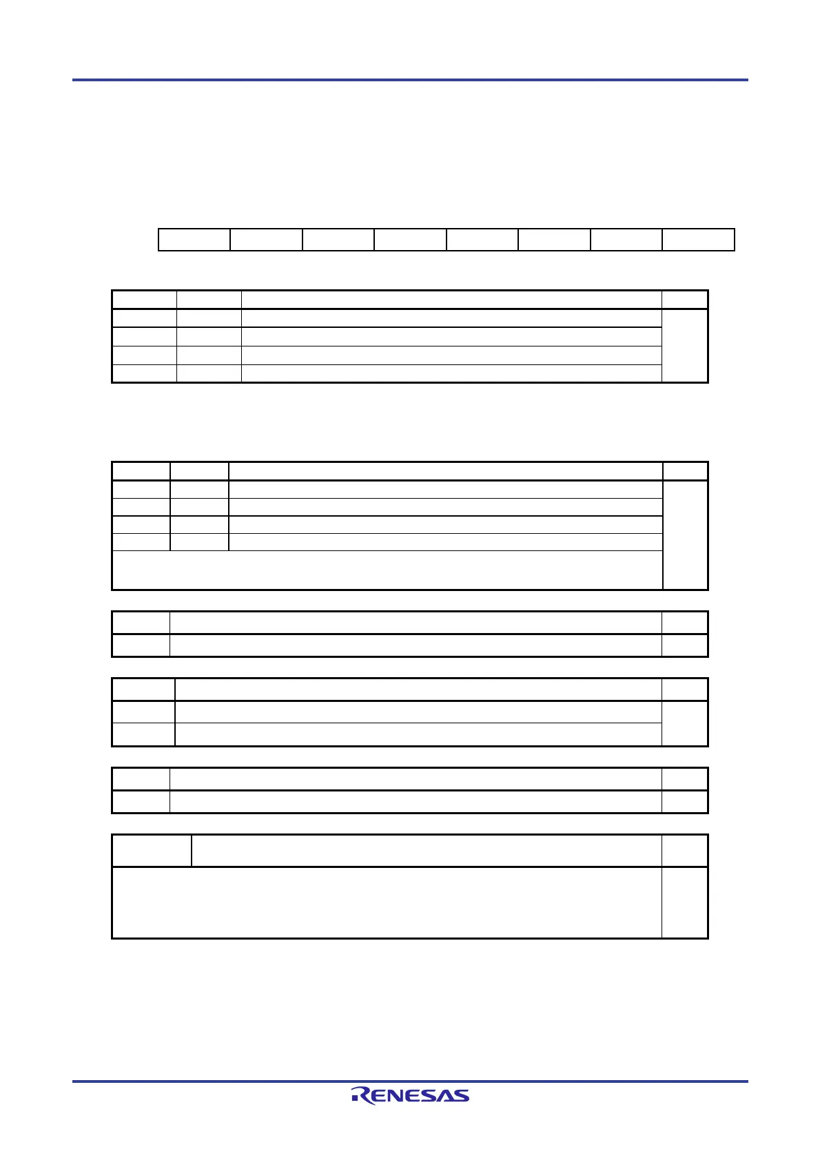
7.3.6 Timer RJ I/O Control Register 0 (TRJIOC0)
Figure 7-7. Format of Timer RJ I/O Control Register 0 (TRJIOC0)
Address : F0241H After Reset: 00H
Symbol 7 6 5 4 3 2 1 0
TRJIOC0 TIOGT1 TIOGT0 TIPF1 TIPF0 — TOENA — TEDGSEL
TIOGT1 TIOGT0
TRJIO0 count control
Notes 1, 2
R/W
0 0 Event is always counted R/W
0 1 Event is counted during polarity period specified for INTP4
1 0 Event is counted during polarity period specified for timer output signal
1 1 Do not set.
Notes 1. When INTP4 or the timer output signal is used, the polarity to count an event can be selected by the
RCCPSEL2 bit in the TRJISR0 register.
2. Bits TIOGT0 and TIOGT1 are enabled only in event counter mode.
TIPF1 TIPF0 TRJIO0 input filter select R/W
0 0 No filter R/W
0 1 Filter sampled at fCLK
1 0 Filter sampled at fCLK/8
1 1 Filter sampled at fCLK/32
These bits are used to specify the sampling frequency of the filter for the TRJIO0 input. If the input to the
TRJIO0 pin is sampled and the value matches three successive times, that value is taken as the input value.
Bit 3 Nothing is assigned R/W
—
The write value must be 0. The read value is 0. R
TOENA TRJO0 output enable R/W
0
TRJO0 output disabled (port)
R/W
1
TRJO0 output enabled
Bit 1 Nothing is assigned R/W
—
The write value must be 0. The read value is 0. R
TEDGSEL I/O polarity switch
R/W
Function varies depending on the operating mode (see Table 7-4 and Table 7-5). The TEDGSEL bit is used
to switch the TRJO0 output polarity and the TRJIO0 I/O edge and polarity. In pulse output mode, only the
inversion/non-inversion of toggle flip-flop is controlled. The toggle flip-flop is initialized when the TRJMR0
register is written or 1 is written to the TSTOP bit in the TRJCR0 register.
R/W
Caution The 20-pin products do not have the timer RJ I/O control register 0 (TRJIOC0).
 Loading...


