RL78/F13, F14 CHAPTER 8 TIMER RD
R01UH0368EJ0210 Rev.2.10 583
Dec 10, 2015
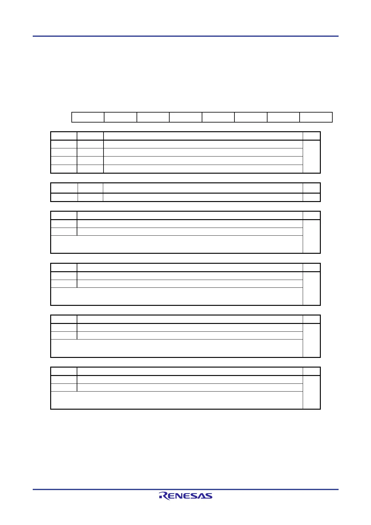
8.2.11 Timer RD Digital Filter Function Select Register i (TRDDFi) (i = 0 or 1)
Figure 8-14. Format of Timer RD Digital Filter Function Select Register i (TRDDFi) (i = 0 or 1)
[Input Capture Function]
Address: F026AH (TRDDF0), F026BH (TRDDF1) After Reset: 00H
Note 1
Symbol 7 6 5 4 3 2 1 0
TRDDFi DFCK1 DFCK0 PENB1 PENB0 DFD DFC DFB DFA
DFCK1 DFCK0
Clock select for digital filter function
Note 2
R/W
0 0 fTRD/32 R/W
0 1 fTRD/8
1 0 fTRD
1 1 Count source (clock selected by bits TCK0 to TCK2 in the TRDCRi register)
PENB1
PENB0
TRDIOBi pin pulse forced cutoff control
R/W
0 0 Set to 00B. R/W
DFD TRDIODi pin digital filter function select R/W
0 Function is not used R/W
1 Function is used
If the digital filter is enabled, edge detection is performed after five or more cycles of the digital filter sampling
clock have elapsed.
DFC TRDIOCi pin digital filter function select R/W
0 Function is not used R/W
1 Function is used
If the digital filter is enabled, edge detection is performed after five or more cycles of the digital filter sampling
clock have elapsed.
DFB TRDIOBi pin digital filter function select R/W
0 Function is not used R/W
1 Function is used
If the digital filter is enabled, edge detection is performed after five or more cycles of the digital filter sampling
clock have elapsed.
DFA TRDIOAi pin digital filter function select R/W
0 Function is not used R/W
1 Function is used
If the digital filter is enabled, edge detection is performed after five or more cycles of the digital filter sampling
clock have elapsed.
Notes 1. The value after reset is undefined when FRQSEL4 = 1 in the user option byte (000C2H/020C2H) and
TRD0EN = 0 in the PER1 register. If it is necessary to read the initial value, set f
CLK to fIH and TRD0EN
= 1 before reading.
2. Set bits DFCK0 and DFCK1 before starting count operation.
 Loading...


