RL78/F13, F14 CHAPTER 8 TIMER RD
R01UH0368EJ0210 Rev.2.10 582
Dec 10, 2015
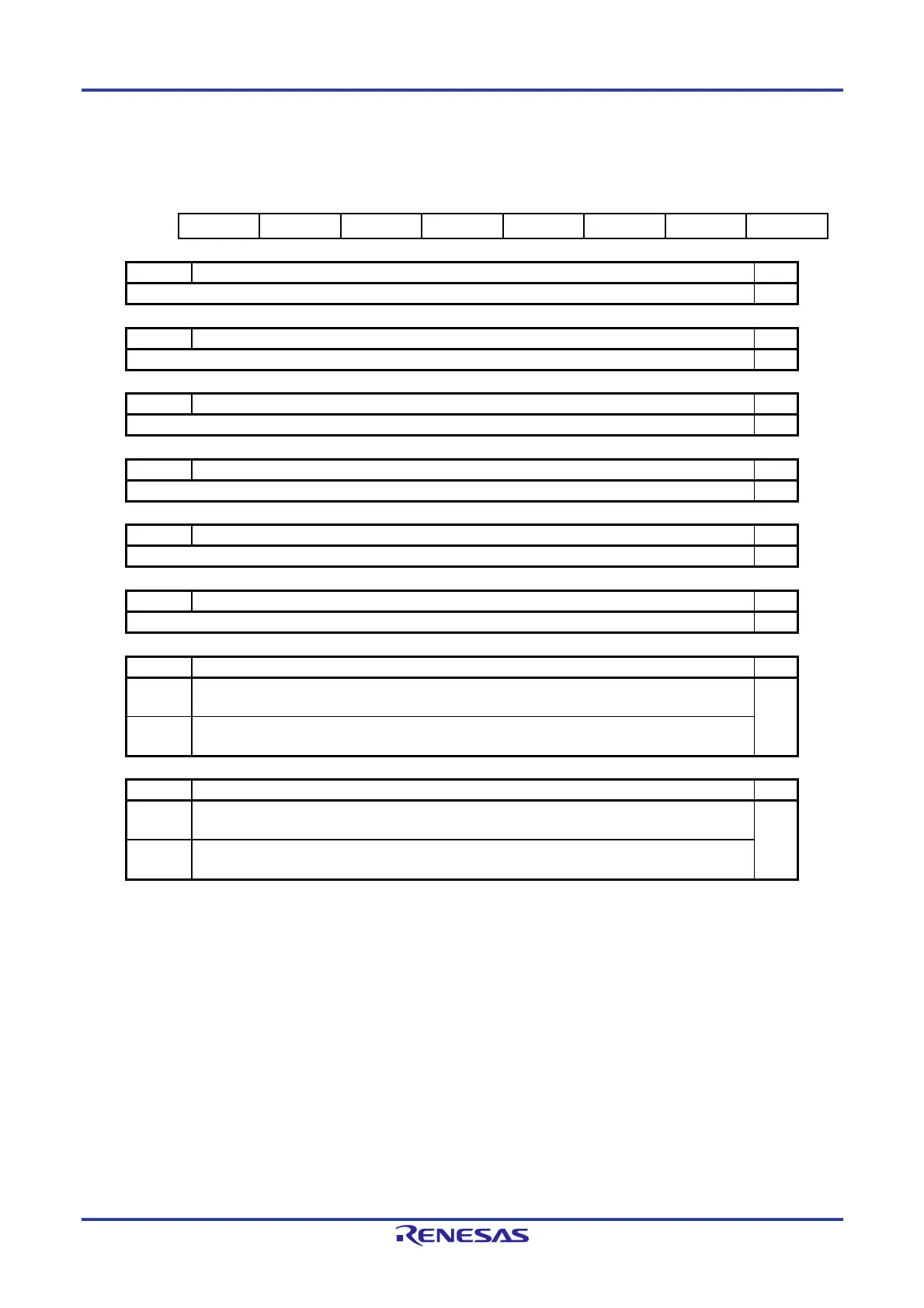
Figure 8-13. Format of Timer RD Output Control Register (TRDOCR) [PWM3 Mode]
Address: F0269H After Reset: 00H
Note 1
Symbol 7 6 5 4 3 2 1 0
TRDOCR TOD1
TOC1 TOB1 TOA1 TOD0
TOC0 TOB0 TOA0
TOD1 TRDIOD1 initial output level select R/W
Disabled in PWM3 mode. R/W
TOC1 TRDIOC1 initial output level select R/W
Disabled in PWM3 mode. R/W
TOB1 TRDIOB1 initial output level select R/W
Disabled in PWM3 mode. R/W
TOA1 TRDIOA1 initial output level select R/W
Disabled in PWM3 mode. R/W
TOD0 TRDIOD0 initial output level select R/W
Disabled in PWM3 mode. R/W
TOC0 TRDIOC0 initial output level select R/W
Disabled in PWM3 mode. R/W
TOB0
TRDIOB0 initial output level select
Note 2
R/W
0 Low initial output, high active level, high output at TRDGRB1 compare match, and low
output at TRDGRB0 compare match
R/W
1 High initial output, low active level, low output at TRDGRB1 compare match, and high
output at TRDGRB0 compare match
TOA0 TRDIOA0 initial output level select
R/W
0 Low initial output, high active level, high output at TRDGRA1 compare match, and low
output at TRDGRA0 compare match
R/W
1 High initial output, low active level, low output at TRDGRA1 compare match, and high
output at TRDGRA0 compare match
Notes 1. The value after reset is undefined when FRQSEL4 = 1 in the user option byte (000C2H/020C2H) and
TRD0EN = 0 in the PER1 register. If it is necessary to read the initial value, set f
CLK to fIH and TRD0EN =
1 before reading.
2. If the pin function is set for waveform output, the initial output level is output when the TRDOCR register
is set.
 Loading...


