RL78/F13, F14 CHAPTER 8 TIMER RD
R01UH0368EJ0210 Rev.2.10 611
Dec 10, 2015
8.2.20 PWM Output Delay Control Register 0 (PWMDLY0)
This register controls output delay of PWM output signal output from the TRDIOj0 and TRDIOj1 pins.
Set the PWMDLY0 register by a 16-bit memory manipulation instruction.
Reset signal generation clears this register to 0000H.
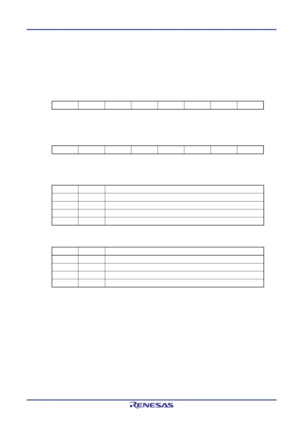
PWMDLY0 register
Address: F0229H After Reset: 00H R/W
15 14 13 12 11 10 9 8
PWMDLY0 TRDD11
Note
TRDD10
Note
TRDC11
Note
TRDC10
Note
TRDB11 TRDB10 TRDA11 TRDA10
Initial value 0 0 0 0 0 0 0 0
R/W R/W R/W R/W R/W R/W R/W R/W R/W
Address: F0228H After Reset: 00H R/W
7 6 5 4 3 2 1 0
PWMDLY0 TRDD01 TRDD00 TRDC01 TRDC00 TRDB01 TRDB00 TRDA01 TRDA00
Initial value 0 0 0 0 0 0 0 0
R/W R/W R/W R/W R/W R/W R/W R/W R/W
Table 8-9. PWM Output Delay Period Control by TRDIOj1 of Timer RD1
TRDj11 TRDj10 PWM Output Delay Control by TRDIOj1 of Timer RD1
0 0 No delay.
0 1 TRDIOj1 signal delayed by one cycle of the timer RD operating clock (fTRD).
1 0 TRDIOj1 signal delayed by two cycles of the timer RD operating clock (fTRD).
1 1 TRDIOj1 signal delayed by three cycles of the timer RD operating clock (fTRD).
j = A, B, C, or D
Table 8-10. PWM Output Delay Period Control by TRDIOj0 of Timer RD0
TRDj01 TRDj00 PWM Output Delay Control by TRDIOj0 of Timer RD0
0 0 No delay.
0 1 TRDIOj0 signal delayed by one cycle of the timer RD operating clock (fTRD).
1 0 TRDIOj0 signal delayed by two cycles of the timer RD operating clock (fTRD).
1 1 TRDIOj0 signal delayed by three cycles of the timer RD operating clock (fTRD).
j = A, B, C, or D
Note If this register is set for a delay, this affects PWM outputs of TRDIOC1 and TRDIOD1, but doesn’t affect the
operation of the timer output signal to internally connected peripheral functions.
Cautions 1. Set the PWMDLY0 register before outputting a PWM signal.
2. Access the PWMDLY0 register in 16 bits. 1-bit access and 8-bit access are prohibited.
3. If this register is not used for PWM output, it should be cleared to 0. This is because the timer output
is delayed by the output delay setting shown above even when the timer output mode other than
PWM output mode is selected.
4. When setting this register after the PWM output is stopped, wait for four cycles of the timer RD
operating clock (f
TRD) before the setting.
5. When using SNZOUT, set TRDC0n to 0 before entering STOP mode (n = 0, 1).
6. Even if this register is set for a delay, this doesn’t affect the operation of other pin functions
multiplexed on the same pin as the TRDIOji pin function (j = A, B, C, D, i = 0, 1).
 Loading...


