RL78/F13, F14 CHAPTER 35 ELECTRICAL SPECIFICATIONS (GRADE K)
R01UH0368EJ0210 Rev.2.10 1754
Dec 10, 2015
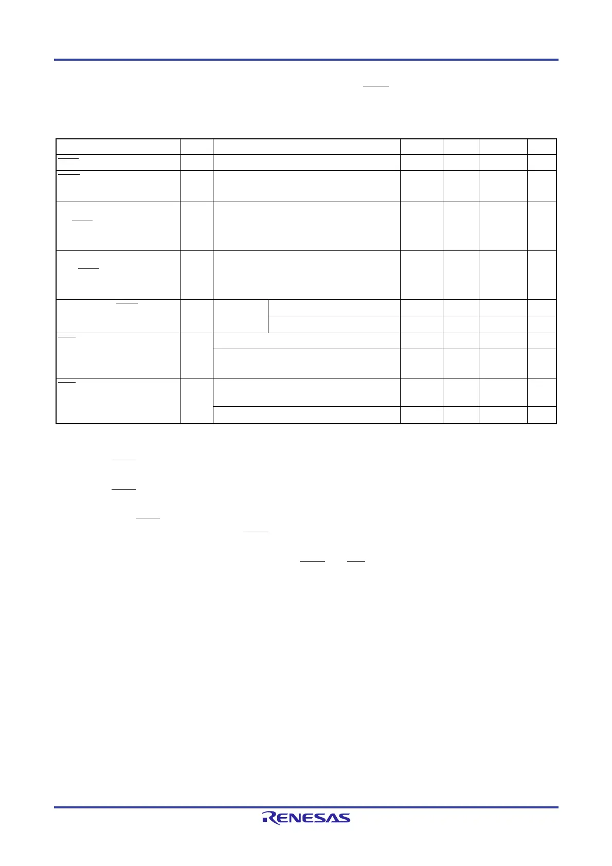
(4) During communication at same potential (CSI mode) (slave mode, SCKp … external clock input, normal slew
rate)
(TA = -40 to +125C, 2.7 V EVDD0 = EVDD1 = VDD 5.5 V, VSS = EVSS0 = EVSS1 = 0 V)
Parameter Symbol Conditions MIN. TYP. MAX. Unit
SCKp cycle time tKCY2
8/f
MCK ns
SCKp high-level width, low-level
width
tKH2,
tKL2
t
KCY2/2 ns
SIp setup time
(to SCKp)
Note 1
tSIK2
1/f
MCK +
20
ns
SIp hold time
(from SCKp)
Note 2
t
KSI2
1/f
MCK +
31
ns
Delay time from SCKp to SOp
output
Note 3
t
KSO2 C = 30 pF
Note 4
4.0V VDD = EVDD0 = EVDD1 5.5V
2/f
MCK + 44 ns
2.7V VDD = EVDD0 = EVDD1 < 4.0V
2/f
MCK + 57 ns
SSIp setup time tSSIK DAP = 0
120 ns
DAP = 1
1/f
MCK +
120
ns
SSIp hold time tKSSI DAP = 0
1/f
MCK +
120
ns
DAP = 1
120 ns
Notes 1. When DAPmn = 0 and CKPmn = 0, or DAPmn = 1 and CKPmn = 1. The Slp setup time becomes "to
SCKp" when DAPmn = 0 and CKPmn = 1 or DAPmn = 1 and CKPmn = 0.
2. When DAPmn = 0 and CKPmn = 0 or DAPmn = 1 and CKPmn = 1. The SIp hold time becomes "from
SCKp" when DAPmn = 0 and CKPmn = 1 or DAPmn = 1 and CKPmn = 0.
3. When DAPmn = 0 and CKPmn = 0, or DAPmn = 1 and CKPmn = 1. The delay time to SOp output becomes
“from SCKp” when DAPmn = 0 and CKPmn = 1, or DAPmn = 1 and CKPmn = 0.
4. C is the load capacitance of the SCKp and SOp output lines.
Caution Select the normal input buffer for the SIp, SCKp and SSIp pins and normal output mode for the SOp
pin.
Remarks 1. p: CSIp (p = 00, 01, 10, 11), m: Unit m (m = 0, 1), n: Channel n (n = 0, 1)
2. f
MCK: Serial array unit operation clock frequency
 Loading...


