RL78/F13, F14 CHAPTER 35 ELECTRICAL SPECIFICATIONS (GRADE K)
R01UH0368EJ0210 Rev.2.10 1761
Dec 10, 2015
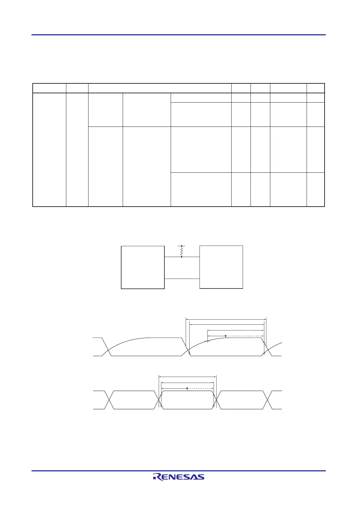
(8) Communication at different potential (UART mode) (TxD output buffer: N-ch open-drain, RxD input buffer:
TTL)
(TA = -40 to +125C, 4.0 V EVDD0 = EVDD1 = VDD 5.5 V, VSS = EVSS0 = EVSS1 = 0 V)
Parameter Symbol Conditions MIN. TYP. MAX. Unit
Transfer rate
Reception 2.7 V Vb EVDD0,
V
IH
= 2.2 V,
V
IL
= 0.8 V
fMCK/6 bps
Theoretical value of the
maximum transfer rate
Note
(C
b = 30 pF)
4.0 Mbps
Transmission 2.7 V Vb EVDD0,
V
OH
= 2.2 V,
V
OL
= 0.8 V
Smaller
number of the
values given
by f
MCK/6 and
expression 1
is applicable.
bps
Theoretical value of the
maximum transfer rate
Note
(C
b = 30 pF)
Normal slew rate
4.0 Mbps
Note Expression 1: Maximum transfer rate = 1 / [{Cb Rb ln (1 2.2/Vb)} 3]
UART mode connection diagram (during communication at different potential)
UART mode bit width (during communication at different potential) (reference)
Caution Select the TTL input buffer for the RxD0 pin and RxD1 pin and N-ch open-drain output mode for the
TxD0 pin and TxD1 pin.
Remarks 1. R
b [Ω]: Communication line (TxD) pull-up resistance, Cb [F]: Communication line (TxD) load capacitance,
Vb [V]: Communication line voltage
2. f
MCK: Serial array unit operation clock frequency
TxD0, TxD1
RxD0, RxD1
Rx
Tx
User's device
Vb
Rb
RL78
microcontroller
TxD0, TxD1
RxD0, RxD1
1/Transfer rate
1/Transfer rate
High-/low-level bit width
Low-level bit width
High-level bit width
Baud-rate tolerance
Baud-rate tolerance
 Loading...


