RL78/F13, F14 CHAPTER 35 ELECTRICAL SPECIFICATIONS (GRADE K)
R01UH0368EJ0210 Rev.2.10 1765
Dec 10, 2015
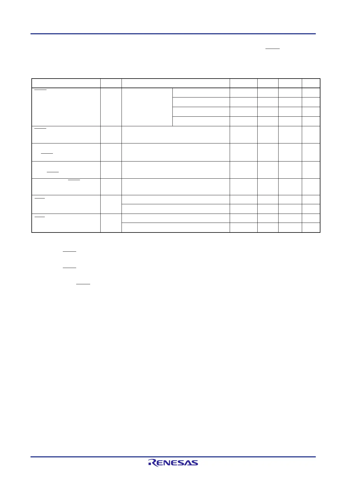
(10) During communication at different potential (3-V supply system) (CSI mode) (slave mode, SCKp … external
clock input, normal slew rate)
(TA = -40 to +125C, 4.0 V EVDD0 = EVDD1 = VDD 5.5 V, VSS = EVSS0 = EVSS1 = 0 V)
Parameter Symbol Conditions MIN. TYP. MAX. Unit
SCKp cycle time tKCY2 2.7 V Vb VDD 20 MHz < fMCK 24 MHz 12/fMCK ns
8 MHz < fMCK 20 MHz 10/fMCK ns
4 MHz < fMCK 8 MHz 8/fMCK ns
fMCK 4 MHz 6/fMCK ns
SCKp high-level width, low-
level width
t
KH2,
t
KL2
2.7 V V
b VDD tKCY2/2 – 20 ns
SIp setup time
(to SCKp)
Note 1
t
SIK2 90 ns
SIp hold time
(from SCKp)
Note 2
t
KSI2
1/f
MCK +
50
ns
Delay time from SCKp to
SOp output
Note 3
t
KSO2
2.7 V V
b VDD,
C
b = 30 pF, Rb = 1.4 kΩ
2/f
MCK +
120
ns
SSIp setup time tSSIK DAP = 0 120 ns
DAP = 1 1/fMCK + 120 ns
SSIp hold time tKSSI DAP = 0 1/fMCK + 120 ns
DAP = 1 120 ns
Notes 1. When DAPmn = 0 and CKPmn = 0, or DAPmn = 1 and CKPmn = 1. The Slp setup time becomes "to
SCKp" when DAPmn = 0 and CKPmn = 1 or DAPmn = 1 and CKPmn = 0.
2. When DAPmn = 0 and CKPmn = 0 or DAPmn = 1 and CKPmn = 1. The SIp hold time becomes "from
SCKp" when DAPmn = 0 and CKPmn = 1 or DAPmn = 1 and CKPmn = 0.
3. When DAPmn = 0 and CKPmn = 0, or DAPmn = 1 and CKPmn = 1. The delay time to SOp output becomes
“from SCKp” when DAPmn = 0 and CKPmn = 1, or DAPmn = 1 and CKPmn = 0.
 Loading...


