RL78/F13, F14 CHAPTER 3 CPU ARCHITECTURE
R01UH0368EJ0210 Rev.2.10 199
Dec 10, 2015
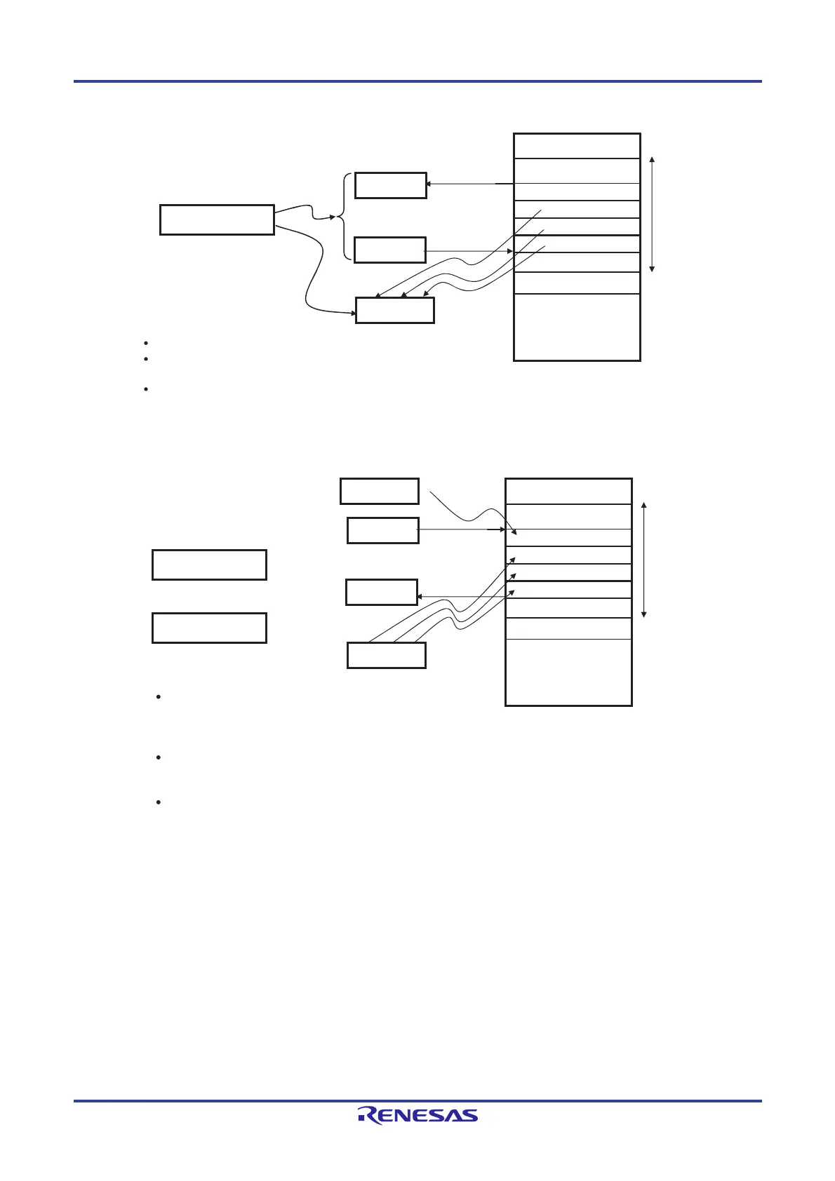
Figure 3-67. Example of RET
Figure 3-68. Example of Interrupt, BRK
RET
SP
(SP+3)
(SP+2)
(SP+1)
(SP)
F0000H
SP+3
SP+2
PC
SP
SP+1
SP
SP+4
Stack
area
Memory
OP-code
<1>
<1>
Instruction code
<2>
<3>
Stack addressing is specified <1>.
The contents of addresses SP, SP + 1, and SP + 2 are stored
in PC bits 7 to 0, 15 to 8, and 19 to 16, respectively <2>.
The value of SP <3> is increased by four.
PSW
SP
SP - 1
PC19 - PC16
PC15 - PC8
PC7 - PC0
SP - 2
SP - 3
SP - 4
F0000H
PC
SP
or
PSW
OP-code
<1>
<2>
<2>
Stack
area
Memory
Instruction code
Interrupt
<3>
Stack addressing is specified <1>. In response to a BRK
instruction or acceptance of an interrupt, the value of the
program counter (PC) changes to indicate the address of
the next instruction.
The values of the PSW, PC bits 19 to 16, 15 to 8, and 7 to
0 are stored in addresses SP - 1, SP - 2, SP - 3, and
SP - 4, respectively <2>.
The value of the SP <3> is decreased by 4.
 Loading...


