RL78/F13, F14 CHAPTER 4 PORT FUNCTIONS
R01UH0368EJ0210 Rev.2.10 354
Dec 10, 2015
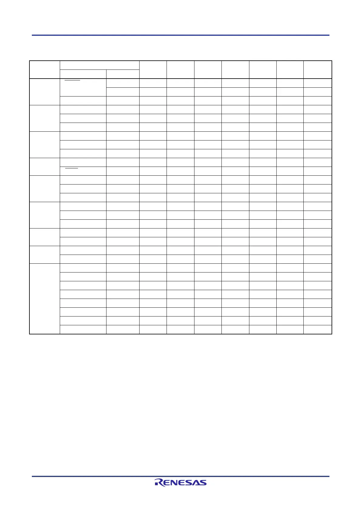
Table 4-29. Settings of Port Mode Register and Output Latch When Using Alternate Function (5/8)
Pin Name Alternate Function PIORXX POMXX PMCXX PMXX PXX PIMXX PITHLXX
Function Name I/O
P60 (SCK00) Input 1 × – 1 × – 0/1
Output 1 0 – 0 1 – ×
(SCL00) Output 1 0/1 – 0 1 – ×
P61 (SI00) Input 1 × – 1 × – 0/1
(SDA00) I/O 1 1 – 0 1 – 0/1
(RXD0) Input 1 × – 1 × – 0/1
P62 SCLA0 I/O × 1 – 0 0 0/1 0/1
(SO00) Output 1 0 – 0 1 × ×
(TXD0) Output 1 0 – 0 1 × ×
P63 SDAA0 I/O × 1 – 0 0 0/1 0/1
(SSI00) Input 1 × – 1 × 0 0/1
P64 (TI14) Input 1 – – 1 × – –
(TO14) Output 1 – – 0 0 – –
(SNZOUT3) Output 1 – – 0 0 – –
P65 (TI16) Input 1 – – 1 × – –
(TO16) Output 1 – – 0 0 – –
(SNZOUT2) Output 1 – – 0 0 – –
P66 (TI00) Input 1 – – 1 × – –
(TO00) Output 1 – – 0 0 – –
P67 (TI02) Input 1 – – 1 × – –
(TO02) Output 1 – – 0 0 – –
P70 ANI26 Input × × 1 1 × × ×
TI15 Input 0 × 0 1 × 0 0/1
SI11 Input 0 × 0 1 × 0/1 0/1
INTP8 Input × × 0 1 × 0 0/1
TO15 Output 0 0 0 0 0 × ×
KR0 Input 0 × 0 1 × 0 0/1
SDA11 I/O 0 1 0 0 1 0/1 0/1
SNZOUT4 Output 0 0 0 0 0 × ×
Remarks 1. : Don't care
PIORxx: Peripheral I/O redirection register
POMxx: Port output mode register
PMCxx: Port mode control register
PMxx: Port mode register
Pxx: Port output latch
2. The relationship between pins and their alternate functions shown in this table indicates the relationship
when a 100-pin product is used. In other products, alternate functions might be assigned to different
pins, but even in this case, the PIORxx, POMxx, PMCxx, PMxx, and Pxx set in the same way.
3. Functions in parentheses in the above table can be assigned via settings in the peripheral I/O
redirection register (PIOR).
(The notes are described after the last table.)
 Loading...