RL78/F13, F14 CHAPTER 5 CLOCK GENERATOR
R01UH0368EJ0210 Rev.2.10 381
Dec 10, 2015
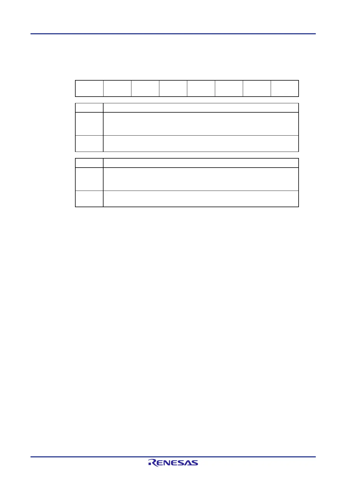
Figure 5-10. Format of Peripheral Enable Register 0 (PER0) (3/3)
Address: F00F0H After reset: 00H R/W
Symbol <7> <6> <5> <4> <3> <2> <1> <0>
PER0 RTCEN 0 ADCEN
IICA0EN
SAU1EN
SAU0EN
TAU1EN
Note
TAU0EN
TAU1EN
Note
Control of timer array unit 1 input clock supply
0
Stops input clock supply.
SFR used by timer array unit 1 cannot be written.
Timer array unit 1 is in the reset status.
1
Enables input clock supply.
SFR used by timer array unit 1 can be read and written.
TAU0EN Control of timer array unit 0 input clock supply
0
Stops input clock supply.
SFR used by timer array unit 0 cannot be written.
Timer array unit 0 is in the reset status.
1
Enables input clock supply.
SFR used by timer array unit 0 can be read and written.
Note Not available in the 20-, 30-, 32-, 48-, and 64-pin products of the RL78/F13 (LIN incorporated)
whose code flash memory is in the range from 16 Kbytes and 64 Kbytes.
 Loading...


