Chapter 10
MSC800
132 Operating instructions | SICK 8011540/14B8/2019-06-06
Subject to change without notice
10.6.2 List of Figures
Fig. 1: MSC800 in combination with ID sensors and external sensors........................ 18
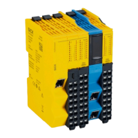
Fig. 2: MSC800-1100 device view (internal view with open door and
view from below) .................................................................................................. 19
Fig. 3: MSC800-2100 device view (internal view with open door and
view from below) .................................................................................................. 20
Fig. 4: MSC800-2300 device view (internal view with open door and
view from below) .................................................................................................. 21
Fig. 5: MSC800-3400 device view (internal view with open door and
view from below) .................................................................................................. 22
Fig. 6: MSC800-3600 device view (internal view with open door and
view from below) .................................................................................................. 23
Fig. 7: MSC800 in combination with ID sensors for 1D / 2D codes on a
conveyor system ................................................................................................... 28
Fig. 8: Diagram of the system (top view) ........................................................................ 28
Fig. 9: Read operating modes (start/stop operation), side reading from above ......... 30
Fig. 10: Read operating modes (tracking operation), side reading from above ............ 31
Fig. 11: Position of the SD memory card for parameter set on the MSC800-0000
logic unit................................................................................................................ 35
Fig. 12: Example of a project-specific dimensional drawing for mounting ..................... 38
Fig. 13: Placement of several ICR890 systems on the conveyor system with
VMS4xx/5xx .......................................................................................................... 39
Fig. 14: Placement of several CLV490 bar code scanners on the conveyor
system ................................................................................................................... 39
Fig. 15: Position of external components ......................................................................... 41
Fig. 16: Block circuit diagram: connection principle for an MSC800 ............................. 44
Fig. 17: Terminals on the MSC800-1100 for mains voltage IN and
supply voltage OUT ............................................................................................... 45
Fig. 18: Terminals on the MSC800-2100 for mains voltage IN and
supply voltage OUT ............................................................................................... 46
Fig. 19: Terminals on the MSC800-2300 for mains voltage IN and
supply voltage OUT ............................................................................................... 47
Fig. 20: Terminals on the MSC800-3400 for mains voltage IN and
supply voltage OUT ............................................................................................... 49
Fig. 21: Terminals on the MSC800-3600 for mains voltage IN and
supply voltage OUT ............................................................................................... 51
Fig. 22: MSC800-0000 logic unit in the cabinet of the MSC800-1100/-2100/
-2300: position of the electrical connections .................................................... 53
Fig. 23: Connecting the cable shields at the inlet to the housing ................................... 59
Fig. 24: Wiring of the HOST data interfaces (terminal block X3)/AUX (terminal
block X9) ............................................................................................................... 65
Fig. 25: Wiring of the CAN interface with termination resistor ........................................ 66
Fig. 26: Block circuit diagram: function of the Ethernet interface .................................. 67
Fig. 27: Wiring of switching input TRIGGER_1 ................................................................. 68
Fig. 28: Wiring of the digital switching output OUT_1 (terminal block X7) ..................... 69