2212 Service Manual
Vertical System
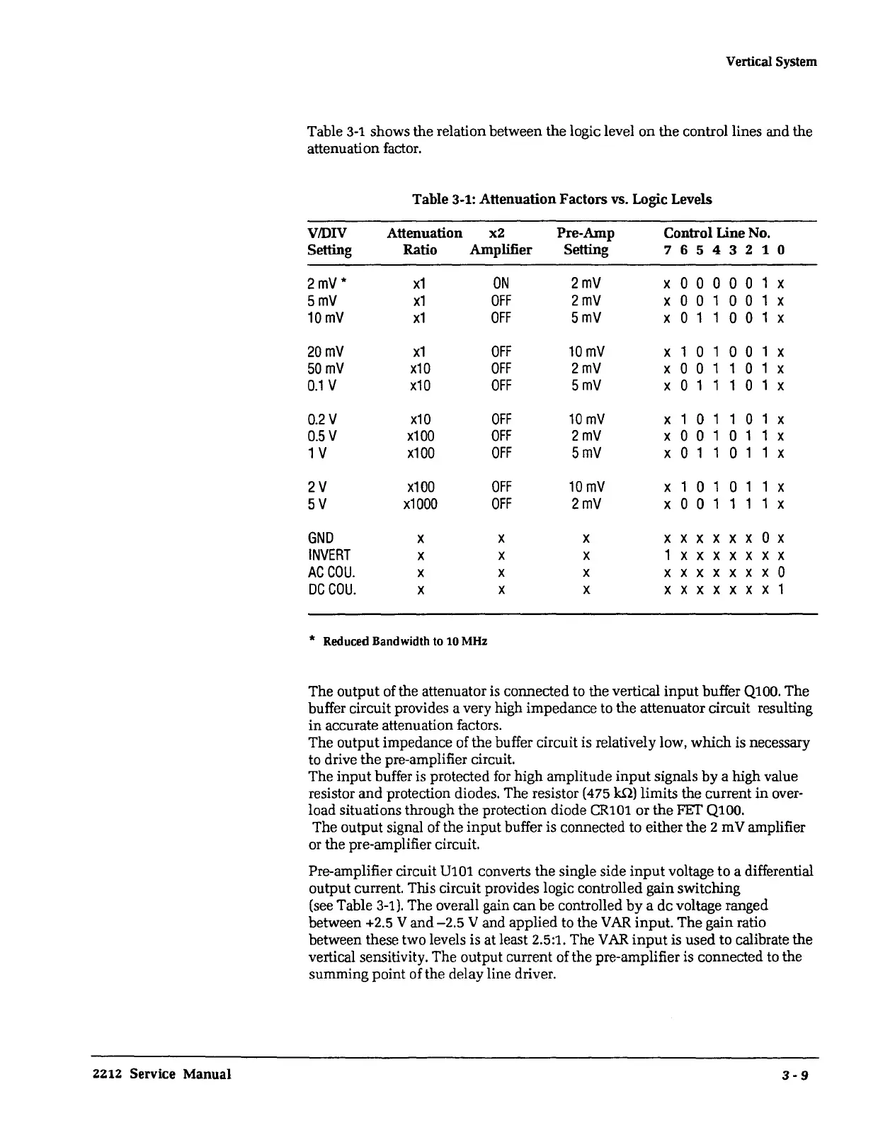
Table
3-1
shows the relation between the logic level
on
the control lines and the
attenuation factor.
Table 3-1: Attenuation Factors vs. Logic Levels
V/DIV
Attenuation x2 Pre-Amp Control Llne No.
Setting
Ratio Amplifier Setting 7 6 5 4 3 2 1 0
2mV*
x1
ON
2mV
x000001
X
SmV
x1
OFF
2mV
x001001x
10mV
x1
OFF
SmV
x011001x
20mV
x1
OFF
10mV
X 1 0 1
0 0
1 X
SOmV
x10
OFF
2mV
X 0 0 1 1 0
1 X
0.1
V
x10
OFF
5mV
X
0 1 1 1 0
1 X
0.2V
x10
OFF
10
mV
X 1 0 1 1 0 1 X
0.5
V
x100
OFF
2mV
X O O 1
0 1 1 X
1V
x100
OFF
5mV
X O 1 1
0 1 1
X
2V
x100
OFF
10mV
X 1 0 1 0 1
1 X
5V
x1000
OFF
2mV
X O O 1
1 1
1 X
GND
X X
X
X X X X X
X
0
X
INVERT
X X X 1 X X X X X X X
AC
GOU.
X X
X
X X X X X X
X
0
DC
GOU.
X
X X
X
X X X X X X 1
* Reduced Bandwidth
to
10
MHz
The output of the attenuator is connected to the vertical
input
buffer Q100. The
buffer circuit provides a very high impedance to the attenuator circuit resulting
in
accurate attenuation factors.
The output impedance of the buffer circuit is relatively low,
which
is necessary
to drive
the
pre-amplifier circuit.
The
input
buffer is protected for high amplitude
input
signals
by
a high value
resistor
and
protection diodes. The resistor (475
kn)
limits the current
in
over-
load situations through the protection diode CR101 or the FET Q100.
The output signal of the
input
buffer is connected to either the 2 m V amplifier
or the pre-amplifier circuit.
Pre-amplifier circuit U101 converts the single side
input
voltage to a differential
output current. This circuit provides logic controlled gain switching
(see Table
3-1).
The overall gain
can
be controlled
by
a de voltage ranged
between +2.5 V and
-2.5
V and applied to the
VAR
input. The gain ratio
between these two levels is at least 2.5:1. The
VAR
input
is used to calibrate the
vertical sensitivity. The output current of the pre-amplifier is connected to the
summing point of the delay line driver.
3-9
 Loading...