Digital
Circuitry
CH
1
...
AID
Convertor
CH1
CH
2
AID
Converter
...
CH2
EXT Clock
Clock
-
Generation
Circuitry
'
j
Acquisition
State Machine
j
3-
26
Acquisition
_
...
-
Acquisition
Ram
-
Bus
Buffer
d0-d7
-
CH1
CH1
"
•
~
Acquisition
...
Acquisition
Ram
-
Bus Buffer
d8-d15
CH2
CH2
V
•
~
Acquisition
68070
Address
---
Microprocesso
Counter
databus
-
Post- Trigger
-
Counter
I
''
•
I
I
Acquisition
d0-d15
I
Control
Latches
-
ACK2_0
REQ2_0
68070 OMA Handshake lines
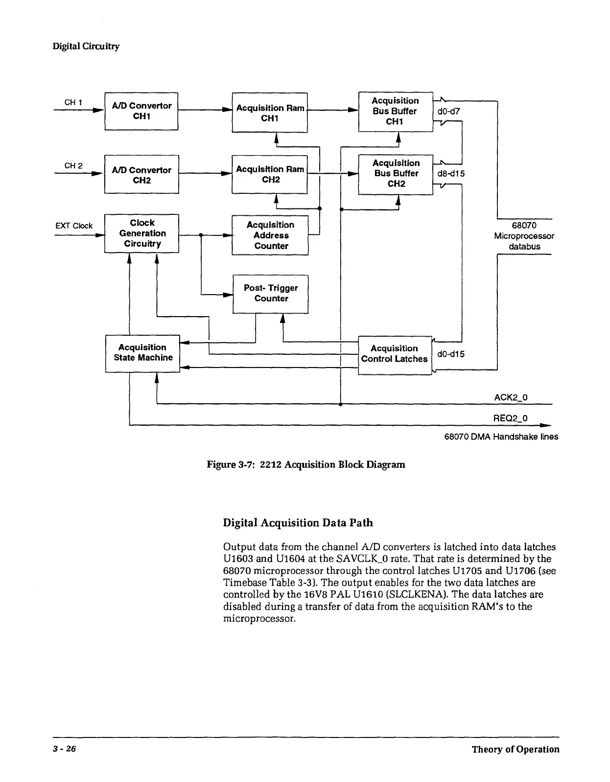
Figure 3-7: 2212 Acquisition Block Diagram
Digital Acquisition Data Path
Output data from the channel
AID
converters is latched into data latches
01603
and 01604 at the
SAVCLK_O
rate. That rate is determined
by
the
68070 microprocessor through the control latches
01705
and
01706
(see
Timebase Table 3-3).
The
output
enables
for
the two data latches are
controlled
by
the 16V8 PAL
01610
(SLCLKENA).
The data latches are
disabled during a transfer of data from the acquisition RAM's to the
microprocessor.
Theory
of
Operation
 Loading...