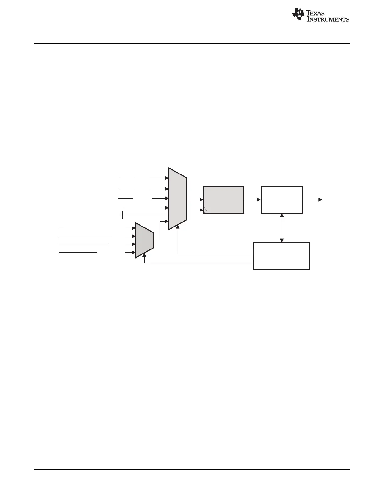
AIN0
. . .
VDD/3
TMP_ SENSOR
AIN7
AVDD
AIN6–AIN7
Decimation
Filter
ClockGeneration
and
Control
AIN7
Input
Mux
Ref
Mux
Sigma-Delta
Modulator
InternalReferenceVoltage
B0304-01
ADC Introduction
www.ti.com
12.1 ADC Introduction
The ADC supports up to 14-bit analog-to-digital conversion with up to 12 bits ENOB (Effective Number Of
Bits). It includes an analog multiplexer with up to eight individually configurable channels and a reference
voltage generator. Conversion results can be written to memory through DMA. Several modes of operation
are available.
The main features of the ADC are as follows:
• Selectable decimation rates which also set the effective resolution (7 to 12 bits).
• Eight individual input channels, single-ended or differential
• Reference voltage selectable as internal, external single-ended, external differential, or AVDD5
• Interrupt request generation
• DMA triggers at end of conversions
• Temperature sensor input
• Battery measurement capability
Figure 12-1. ADC Block Diagram
12.2 ADC Operation
This section describes the general setup and operation of the ADC and describes the use of the ADC
control and status registers accessed by the CPU.
12.2.1 ADC Inputs
The signals on the port-0 pins can be used as ADC inputs. In the following, these port pins are referred to
as the AIN0–AIN7 pins. The input pins AIN0–AIN7 are connected to the ADC.
It is possible to configure the inputs as single-ended or differential inputs. In the case where differential
inputs are selected, the differential inputs consist of the input pairs AIN0–AIN1, AIN2–AIN3, AIN4–AIN5,
and AIN6–AIN7. Note that no negative supply can be applied to these pins, nor a supply higher than VDD
(unregulated power). It is the difference between the pins of each pair that is converted in differential
mode.
In addition to the input pins AIN0–AIN7, the output of an on-chip temperature sensor can be selected as
an input to the ADC for temperature measurements. In order to do so, the registers TR0.ADCTM and
ATEST.ATESTCTRL must be set as described in the register descriptions in Section 12.2.10 and
Section 23.15.3 (CC253x) or Section 24.1 (CC2540), or Section 25.12 (CC2541).
It is also possible to select a voltage corresponding to AVDD5/3 as an ADC input. This input allows the
implementation of, e.g., a battery monitor in applications where this feature is required. Note that the
reference in this case must not be dependent on the battery voltage; for instance, the AVDD5 voltage
must not be used as a reference.
138
ADC SWRU191C–April 2009–Revised January 2012
Submit Documentation Feedback
Copyright © 2009–2012, Texas Instruments Incorporated

 Loading...


