www.ti.com
CPU Registers
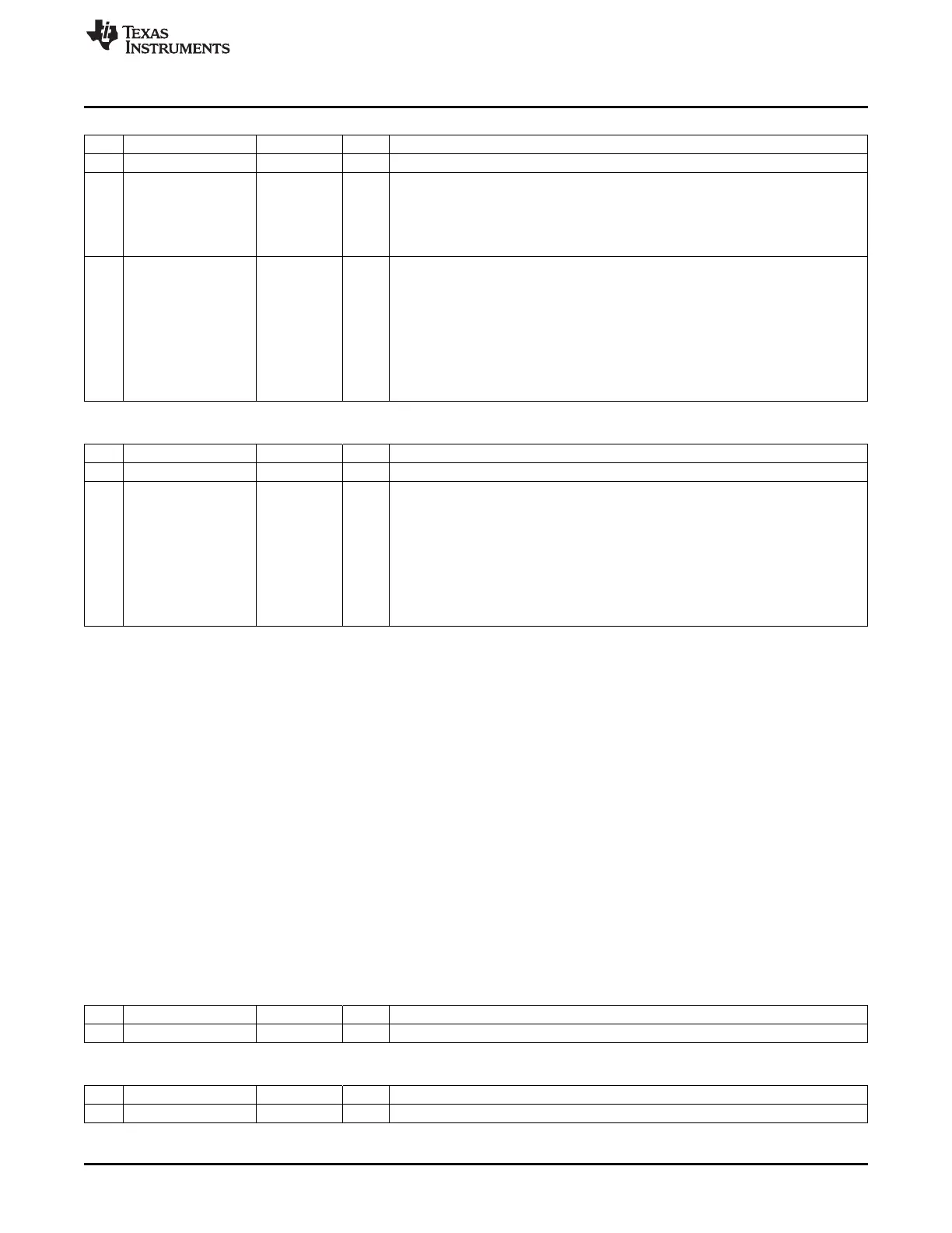
MEMCTR (0xC7) – Memory Arbiter Control
Bit Name Reset R/W Description
7:4 — 0000 R0 Reserved
3
XMAP
0 R/W XDATA map to code. When this bit is set, the SRAM XDATA region, from 0x0000
through (SRAM_SIZE – 1) is mapped into the CODE region from 0x8000 through
(0x8000 + SRAM_SIZE – 1). This enables execution of program code from RAM.
0: SRAM map into CODE feature disabled
1: SRAM map into CODE feature enabled
2:0
XBANK[2:0]
000 R/W XDATA bank select. Controls which code bank of the physical flash memory is
mapped into the XDATA region (0x8000–0xFFFF). When set to 0, the root bank is
mapped in.
Valid settings depend on the flash size for the device. Writing an invalid setting is
ignored, i.e., no update to XBANK[2:0] is performed.
32-KB version: 0 only (i.e, the root bank is always mapped in.)
64-KB version: 0–1
96-KB version: 0–2
128-KB version: 0–3
256-KB version: 0–7
FMAP (0x9F) – Flash Bank Map
Bit Name Reset R/W Description
7:3 — 0000 0 R0 Reserved
2:0
MAP[2:0]
001 R/W Flash bank map. Controls which bank is mapped into the bank area of the CODE
memory space (0x8000–0xFFFF). When set to 0, the root bank is mapped in. Valid
settings depend on the flash size for the device. Writing an invalid setting is ignored,
i.e., no update to MAP[2:0] is performed.
32-KB version: No value can be written. Bank area is only used for running program
code from SRAM. See MEMCTR.XMAP.
64-KB version: 0–1
96-KB version: 0–2
128-KB version: 0–3
256-KB version: 0–7
2.3 CPU Registers
This section describes the internal registers found in the CPU.
2.3.1 Data Pointers
Two data pointers, DPTR0 and DPTR1, exist to accelerate the movement of data blocks to/from memory.
The data pointers are generally used to access CODE or XDATA space. For example:
MOVC A,@A+DPTR
MOV A,@DPTR.
The data pointer select bit, bit 0 in the data pointer select register DPS, chooses which data pointer is the
active one during execution of an instruction that uses the data pointer, e.g., in one of the preceding
instructions.
The data pointers are two bytes wide, consisting of the following SFRs:
• DPTR0–DPH0:DPL0
• DPTR1–DPH1:DPL1
DPH0 (0x83) – Data Pointer-0 High Byte
Bit Name Reset R/W Description
7:0
DPH0[7:0]
0x00 R/W Data pointer-0, high byte
DPL0 (0x82) – Data Pointer-0 Low Byte
Bit Name Reset R/W Description
7:0
DPL0[7:0]
0x00 R/W Data pointer-0, low byte
37
SWRU191C–April 2009–Revised January 2012 8051 CPU
Submit Documentation Feedback
Copyright © 2009–2012, Texas Instruments Incorporated

 Loading...


