BSP_MODE.W_PN9_EN
B0467-01
Output
s
8
b
0
b
1
b
2
b
3
b
4
b
5
b
6
b
7
s
7
s
6
s
5
s
4
s
3
s
2
s
1
s
0
PN9 Whitening
Bit-Stream Processor
www.ti.com
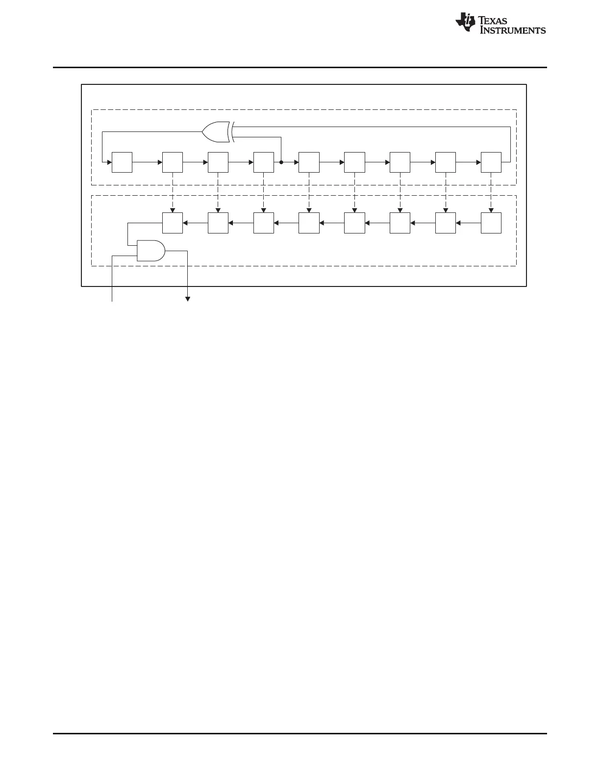
Figure 25-4. CC2500-Compatible Whitening
25.4.3 CRC
A block diagram showing the operation of the CRC module is given in Figure 25-5. The CRC sub-module
has two registers:
• A 32-bit data shift register d
• A 32-bit register p for holding the polynomial
The p register defines the shift register used for calculating CRC. There is a feedback tap in the locations
where the corresponding bit of p is set to 1. The module input is XORed by the output of the shift register,
and this becomes the feedback of the shift register.
The current value of the data shift register d is the CRC value. Prior to the start of CRC calculation, the d
and p registers should be initialized by writing d to registers BSP_D[0–3] and p to registers
BSP_P[0–3]. The BSP_P[0–3] registers only must be set once, whereas the BSP_D[0–3] registers
should be set again for each packet. In normal transmit and receive modes, this is handled by the LLE,
which writes the value of PRF_CRC_INIT[0–3] to BSP_D[0–3]. At the end of CRC calculation, the value
of the register is serially shifted out on the output. When performing CRC checking, all the BSP_D[0–3]
registers should be 0 for the CRC to be OK after the received CRC has been fed through the shift register.
If whitening is enabled, calculated CRC bytes are whitened before transmission, and received CRC bytes
are de-whitened before CRC checking.
306
CC2541 Proprietary Mode Radio SWRU191C– April 2009–Revised January 2012
Submit Documentation Feedback
Copyright © 2009–2012, Texas Instruments Incorporated

 Loading...


