Registers
www.ti.com
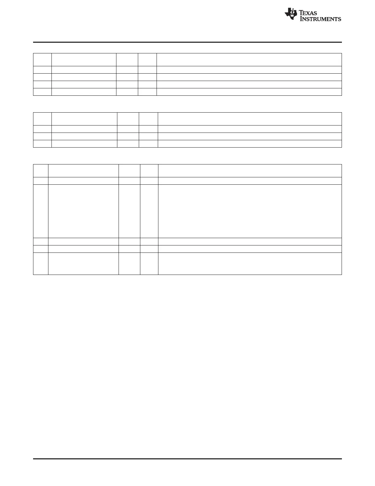
ADCTEST0 (0x61B5) – ADC Tuning
Bit Name Reset R/W Description
No.
7:6
ADC_VREF_ADJ[1:0]
00 R/W Quantizer threshold control for test/debug
5:4
ADC_QUANT_ADJ[1:0]
01 R/W Quantizer threshold control for test/debug
3:1
ADC_GM_ADJ[2:0]
000 R/W Gm control for test/debug
0
ADC_DAC2_EN
0 R/W Enables DAC2 for enhanced ADC stability
ADCTEST1 (0x61B6) – ADC Tuning
Bit Name Reset R/W Description
No.
7:4
ADC_TEST_CTRL[3:0]
0000 R/W ADC test mode selector
3:2
ADC_C2_ADJ[1:0]
11 R/W Used to adjust capacitor values in ADC
1:0
ADC_C3_ADJ[1:0]
10 R/W Used to adjust capacitor values in ADC
ADCTEST2 (0x61B7) – ADC Tuning
Bit Name Reset R/W Description
No.
7 – 0 R0 Reserved. Read as 0
6:5
ADC_TEST_MODE
00 R/W Test mode to enable output of ADC data from demodulator. When enabled, raw
ADC data is clocked out on the GPIO pins.
00: Test mode disabled
01: Data from both I and Q ADCs is output, data rate 76 MHz
10: Data from I ADC is output. Two and two ADC samples grouped, data rate
38 MHz
11: Data from Q ADC is output. Two and two ADC samples grouped, data rate
38 MHz
4:3
AAF_RS[1:0]
00 R/W Controls series resistance of AAF
2:1
ADC_FF_ADJ[1:0]
01 R/W Adjust feedforward
0
ADC_DAC_ROT
1 R/W Control of DAC DWA scheme
0: DWA (scrambling) disabled
1: DWA enabled
280
CC253x Radio SWRU191C–April 2009–Revised January 2012
Submit Documentation Feedback
Copyright © 2009–2012, Texas Instruments Incorporated

 Loading...


