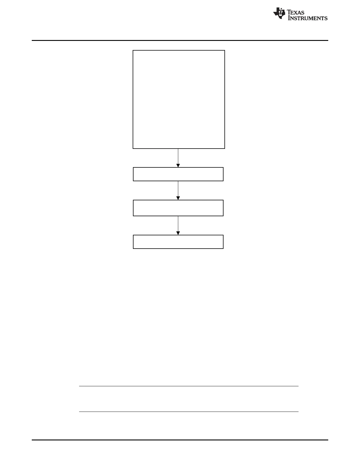
SetupDMAchannel:
SRCADDR=<XDATAlocation>
DESTADDRR=FWDATA
VLEN=0
LEN=<blocksize>
WORDSIZE=byte
TMODE=singlemode
TRIG=FLASH
SRCINC=1byte
DESTINC=0bytes
IRQMASK=yes
M8=0
PRIORITY=high
ArmDMAChannel
Startflashwrite
Setupflashaddress
F0031-01
Flash Page Erase
www.ti.com
Figure 6-1. Flash Write Using DMA
6.2.4 CPU Flash Write
To write to the flash using the CPU, a program executing from SRAM must implement the steps outlined
in the procedure described in Section 6.2.1. Disable interrupts to ensure the operation does not time out.
6.3 Flash Page Erase
The flash page-erase operation sets all bits in the page to 1.
A page erase is initiated by setting FCTL.ERASE to 1. The page addressed by FADDRH[7:1]
(CC2530/CC2531/CC2540/CC2541) or FADDRH[6:0] (CC2533) is erased when a page erase is initiated
. Note that if a page erase is initiated simultaneously with a page write, i.e., FCTL.WRITE is set to 1, the
page erase is performed before the page-write operation starts. The FCTL.BUSY bit can be polled to see
when the page erase has completed.
Power mode 1, 2, or 3 must not be entered while erasing a page. Also, the system clock source
(XOSC/RCOSC) must not be changed while erasing.
NOTE: If a flash page-erase operation is performed from within flash memory and the Watchdog
Timer is enabled, a Watchdog Timer interval must be selected that is longer than 20 ms, the
duration of the flash page-erase operation, so that the CPU can clear the Watchdog Timer.
78
Flash Controller SWRU191C– April 2009–Revised January 2012
Submit Documentation Feedback
Copyright © 2009–2012, Texas Instruments Incorporated

 Loading...


