Assembly Removal and Replacement, MS203xC 7-25 Installing Main PCB and Reassembling Instrument
MS20xxC MM PN: 10580-00307 Rev. D 7-73
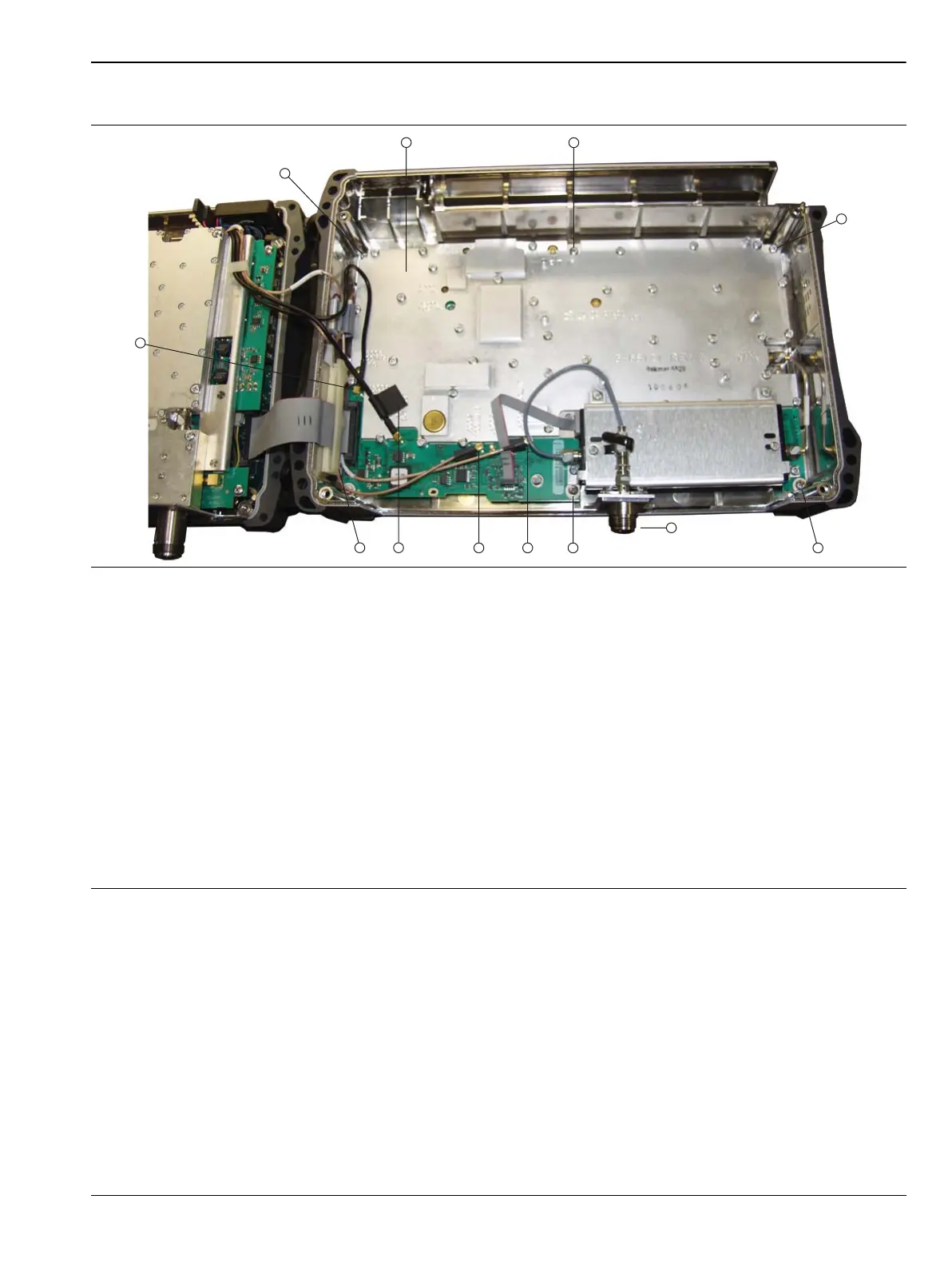
15. Snap open the cable clip in the back case (item 13 in Figure 7-39), and insert the four single RF cables
from the Mother Board and the VNA PCB Assembly to the SPA PCB at MMCX connectors J6000, J6001,
J6002, and J4004.
a. J6000 (item 9 in Figure 7-38) is for the External Reference cable from the Ext. Ref. connector on
the top connector panel (attached to the VNA Assembly).
b. J6001 (item 11 in Figure 7-38) is for the 10 MHz Ref Out connector on the top connector panel
(attached to the VNA Assembly).
c. J6002 (item 8 in Figure 7-38) is for the 100 MHz In connector. The other end is connected to J2200
on the Mother Board (item 8 in Figure 7-35 on page 7-70).
1. PCB
2. Screw (1 of 6 holding PCB to case back)
3. Screw (1 of 6 holding PCB to case back)
4. Screw (1 of 6 holding PCB to case back)
5. SPA RF In Connector (protrudes through connector panel of VAN Assembly when instrument is assembled)
6. Screw (1 of 6 holding PCB to case back)
7. MMCX Connector J4004, 140 MHz IF
8. Connector J6002, 100 MHz to MB (Mother Board)
9. Connector J6000, External Reference In
10.Screw (1 of 6 holding PCB to case back)
11.Connector J6001, 10 MHz Reference Out, located adjacent to J5006 (for ribbon cable)
12.Screw (1 of 6 holding PCB to case back)
Figure 7-38. SPA PCB in Case Back – Cables Connected
 Loading...